Abstract: Based on the important role of optical switch in optical transmission and exchange, this paper briefly introduces the hardware connection of optical switch drive circuit, focusing on the FPGA implementation method of optical switch operation timing.
0 Introduction Optical switches are devices that convert optical signals from one optical channel to another as required. With the increase of the capacity and speed of the communication network, the establishment of the All OpTIcal Network (AON) has become the development direction of communication technology. One of the main features of all-optical network [1-2] is the wide application of optical add/drop multiplex (OADM) and optical cross-connect (OXC) modules. Optical switches are the core components of OADM and OXC, developing high performance and low cost. Optical switches and optical switch modules are of great significance for the development of optical fiber communication technology. Optical switches are more important passive optical devices, eliminating the need for optical/electrical, electrical/optical conversion processes, simplifying equipment, improving network reliability, and providing a flexible signal routing platform. The function of the optical switch includes the on and off of the signal in the same channel, the wavelength conversion of the optical signal in the same channel, and the conversion of the optical signal between different channels.
In addition to the design principle and structure of the optical switch module itself, its control and drive circuit is also an important factor affecting the performance of the optical switch module [3-4]. At present, the optical switch control system [5-10] is usually implemented by a single-chip microcomputer, and the corresponding program of a PC simulates local control and sends corresponding routing information. The information of the PC is sent to the MCU through the serial port, and the MCU performs further control actions. The information such as the success or failure of the MEMS optical switch is read by the microcontroller and the control data in its internal register is compared with the original correct data. After the operation is completed, the MCU generates corresponding feedback information to the PC through the serial port.
This paper presents an FPGA design method for the optical switch module control circuit. The channel is set by hardware, the channel information is read by the FPGA, decoded, and sent to the drive circuit of the optical switch. The optical switch channel switching success flag information is obtained by comparing the status signal fed back by the optical switch with the original data read by the FPGA: If the two are the same, the channel switching is correct, and if the two are different, the channel switching error occurs.
Implementing an ASIC with FPGA can not only modify and implement various logic functions quickly and flexibly, but also simplify interface and control, which is beneficial to improve the overall performance and reliability of the system, and at the same time meet various high speeds. Design speed requirements. In addition, in the actual use process, if the product has hardware problems in the customer or needs to be upgraded, there is no need to re-develop the product, just let the customer download a program, which saves the after-sales maintenance and upgrade cost.
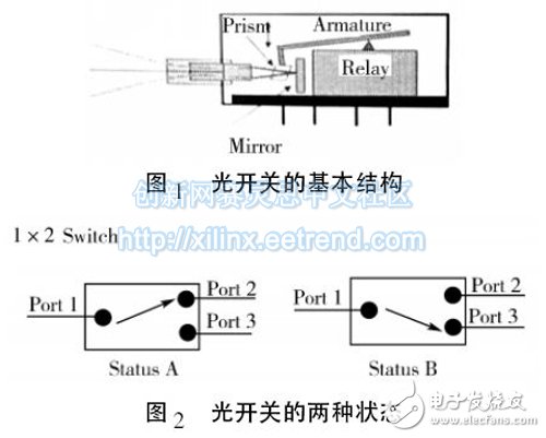
1, 1 & TImes; 8 optical switch module basic structure and working principle 1. 1 MEMS 1 &TImes; 2 basic structure of optical switchMEMS optical switches [11-12] use MEMS technology to engrave a number of tiny lenses on silicon crystals. By electrostatic or electromagnetic forces, the movable micromirrors can be lifted, rotated or moved to change the input light. The direction of propagation to achieve the function of light path on and off. As shown in Figure 1 and Figure 2: MEMS 1 & TImes; 2 The optical switch consists of a tiny mirror and relay controlled by static electricity. The arrangement of the beam in the two-dimensional space of the micromirror has only two states, that is, through the two states of channel 2 or channel 3. In the control circuit, as long as sufficient driving voltage is provided to operate the relay and then deflect the micromirror, the channel for optical transmission can be changed [13].
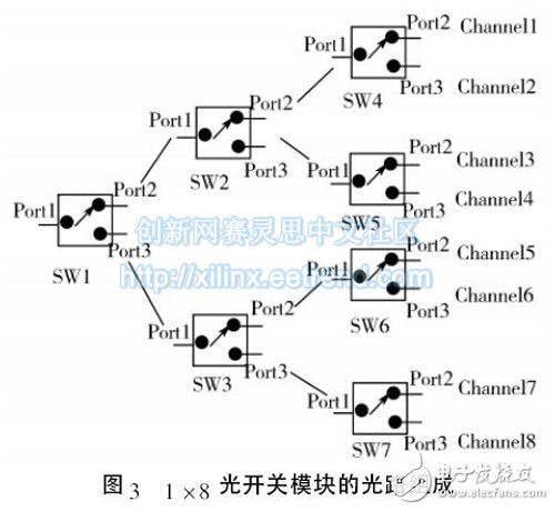
The MEMS 1 × 8 optical switch is a cascade of three sets of 1 × 2 optical switches. As shown in Figure 3, the function of this module is that light enters from Port1 of SW1 and can be output from any channel in Channel1-Channel8.
The overall structure of the optical opening module circuit is shown in Figure 4. The whole circuit is mainly divided into three modules: FPGA control module, optical switch drive circuit, and 1 × 8 optical switch module.
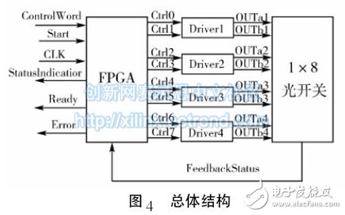
(1) FPGA control module: This module mainly realizes the functions of optical switch operation timing, input channel decoding, and optical switch channel selection error.
The following describes the signals of the module:
ControlWord: Select the control word for the channel, which can be done manually.
Start: Start signal, active low, that is, the optical switch performs channel switching.
StatusIndication: Status indication signal indicating whether the status signal fed back to the FPGA after the drive circuit is consistent with the required channel. If not, the alarm is processed.
CLK: The clock input to the FPGA, where CLK is 3. 17kHz.
Ready: The flag from the beginning to the end of the conversion.
Error: The flag of the channel conversion is correct or not.
Ctrl0-Ctrl7: Decoded signal of the FPGA.
(2) Optical switch drive circuit: The drive circuit mainly performs current amplification on the decoding signal of the channel to convert it into a signal capable of driving the optical switch, as shown in FIG.
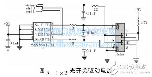
In Figure 5, Ctrl0 and Ctrl1 are the control signals input to the FPGA, the control signals are loaded into the drive circuit, and the pulsed electrical signals are output.
The OUTa and OUTb control relays are turned on or off, and then the rotation of the micromirror is driven to select the light output channel. Status is the status signal for feedback.
In the 1 × 8 optical switch module, four sets of drive circuits are used to amplify the channel's decoded signal. OUTa1 and OUTb1 drive SW1, OUTa2 and OUTb2 drive SW2 and SW3, OUTa3 and OUTb3 drive SW4 and SW5, and OUTa4 and OUTb4 drive SW6. And SW7.
(3) 1 × 8 optical switch module: After receiving the drive signal, channel selection is performed to output the input light from the set channel.
The basic principle of the whole control circuit is: manually set the serial number of the optical channel, press the Start (start signal) optical switch to work, perform channel switching, and the FPGA module translates the set channel signal into a driving signal through the driving circuit to the optical switch. Take control. Finally, the optical switch feeds back to the FPGA its current state information, and the FPGA compares it with the set channel signal. If the same, the channel switch succeeds, Error is low; if not, the channel switch fails, Error is High level.
2. 2 FPGA clock selectionThe clock circuit is shown in Figure 6.
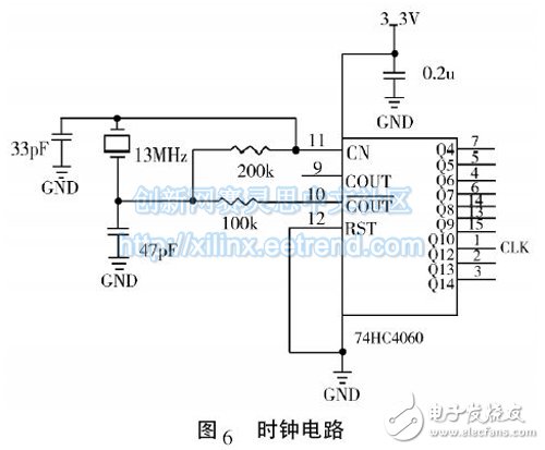
The clock signal is realized by a 14-bit counter. In this circuit, the crystal oscillator is 13MHz, and Q12 is used as the input signal of the clock CLK of the FPGA. At this time, the frequency = 13MHz /2^12 = 3. 17kHz. It takes about 10ms to wait for the switching action to be formed by the FPGA. As long as a counting program is designed in the software program, counting from 0 to 31, that is, the waiting time = (1 / 3.17) * 32 = 10ms, the waiting time of 10ms Then formed.
2. 3 optical switch channel selection truth tableThe optical switch channel selection signal truth table is shown in Figure 7.
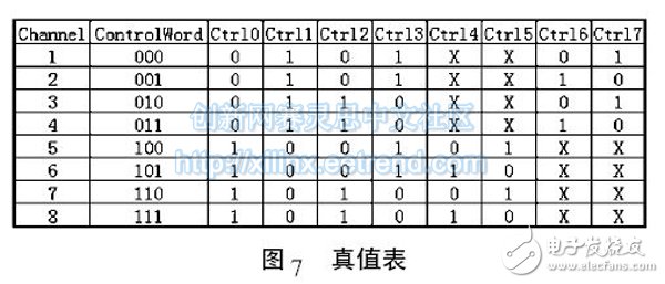
ControlWord is the set channel, Ctrl0-Ctrl7 is the decoding signal of the FPGA to the channel is added to the drive circuit, and Status1-Status4 is used as the feedback status signal.
2. 4 FPGA implementation of optical switch control timingAn important parameter for the operation of the optical switch is the switch speed (Switch Speed), which reflects the speed of the switch switching channel process. In this design, an optical switch with a switch response speed of about 10 ms is selected. To achieve the control process of the entire optical switch, the following timing is designed, as shown in FIG.
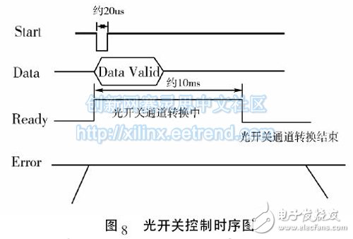
In Figure 8, Start is the start signal, active low, Data is the optical switch channel signal, that is, the decoding signal of ControlWord, Ready is the start and end of the optical switch channel switching, Error is used to indicate whether the channel switching is correct, “0†"" indicates an error, and "1" indicates correct.
2. 5 optical switch channel switching state diagramThe optical switch channel switching state diagram [14] is shown in Figure 9.
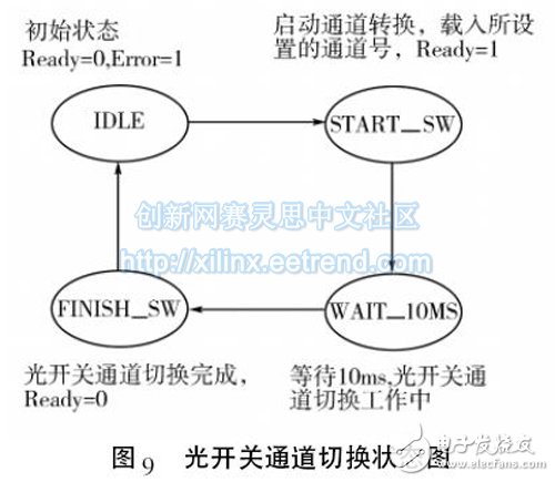
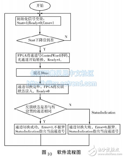
The state diagram is divided into 4 states: IDLE, START _ SW, WAIT_10MS, FINISH_SW. The initial state is IDLE before the start signal is pressed. At this time, the decoding signal bits of the channel are all 0, and Ready = 0, Convert_Falg = 0, and Error = 1. When the start signal is pressed, the state goes to START_SW. At this time, the optical switch starts to switch channels, and the set channel number (ControlWord) is decoded into a drive signal by the FPGA and then sent to the drive and then sent to the optical switch module, and at this time, the optical switch 4 The 9 pin is fed back to the FPGA as a status bit. Simultaneously set Ready = 1, Convert_Falg = 1, and then wait for about 10ms, that is, enter state WAIT_10MS, wait for completion to enter FINISH_SW, then the channel switch is completed, set Ready = 0, Convert_Flag = 0.
In addition, when the optical switch channel is switched, the FPGA compares the feedback back state with the previously set channel signal. If it is inconsistent, set Error = 0, otherwise Error = 1.
2. 6 FPGA module software implementationThe program uses the Verilog HDL language, and the flowchart is shown in Figure 10.
The simulation results are shown in Figure 11.
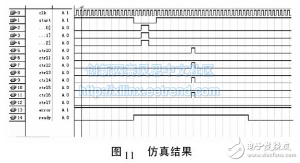
From the simulation results, it can be seen that when the channel is set to channel8, the corresponding drive signals ctrl0 to ctrl7 are 101001010, which is consistent with the truth table, and the Ready and Error signals of the output also meet the timing requirements.
4 ConclusionThis paper introduces the overall structure of the MEMS 1 × 8 optical switch module, elaborates the specific application of the FPGA in the optical switch module control circuit, analyzes how the FPGA works with the optical switch response speed to generate the optical switch's working sequence, and analyzes how to A method of decoding a channel into an optical switch drive signal. The overall structure of the control circuit is simple, which is beneficial to improve the overall performance and reliability of the system, and at the same time can well meet the speed requirements of various high-speed designs.
Bitmain Antminer Asic Miner:Bitmain Antminer Z15,Bitmain Antminer Z9 Mini,Bitmain Antminer Z9,Bitmain Antminer Z11
Bitmain is the world's leading digital currency mining machine manufacturer. Its brand ANTMINER has maintained a long-term technological and market dominance in the industry, with customers covering more than 100 countries and regions. The company has subsidiaries in China, the United States, Singapore, Malaysia, Kazakhstan and other places.
Bitmain has a unique computing power efficiency ratio technology to provide the global blockchain network with outstanding computing power infrastructure and solutions. Since its establishment in 2013, ANTMINER BTC mining machine single computing power has increased by three orders of magnitude, while computing power efficiency ratio has decreased by two orders of magnitude. Bitmain's vision is to make the digital world a better place for mankind.
Bitmain Antminer Asic Miner,Z15 bitmain antminer,Z11 Antminer Bitmain,zcash miner,zec mining machine
Shenzhen YLHM Technology Co., Ltd. , https://www.ylhm-tech.com