Abstract: DS33R41 is an inverse multiplexed Ethernet mapper with a T1 / E1 / J1 transceiver. This application note describes how to change the netlist of a printed circuit board (PWB) for a design using DS33R41 to make it conform to the JTAG specification . Because the DS33R41 is a multi-chip module that contains multiple chips in a package, the boundary scan description language (BSDL) used for board-level joint test action group (JTAG) testing cannot define this situation, so these Changes are necessary. This application note contains the external pin mapping table, internal chip pad binding table, and the connection information required by the designer to quickly complete the correct JTAG boundary scan test.
Overview In the hardware manufacturing of telecommunication systems, one of the most basic tasks is to check for any production defects that may be contained in the system. Among the many hardware testing methods, one of the most commonly used methods is to use the Joint Test Action Group (JTAG) boundary scan method. The boundary scan test method will make some minor changes to the hardware before production, so hardware verification can be performed after production. In the design process, all integrated circuits (ICs) that support JTAG are connected in series in a daisy chain through the JTAG test interface, and verification is completed by a special JTAG test system connected to the test interface. The JTAG test system uses a printed circuit board ( PWB) Netlist, Boundary Scan Description Language (BSDL) files, and PWB connection test vectors verify point-to-point connections.
BSDL testing is simple. However, for multi-chip module devices, such as the inverse multiplexed Ethernet mapper DS33R41 with T1 / E1 / J1 transceivers, there is no way to include them in the BSDL file because they contain multiple die dies in one package Describe these devices correctly, but you can overcome this shortcoming by making minor changes to the PWB netlist and using two BSDL files to describe the device package.
Adjusting the netlist of the printed circuit board Before the JTAG boundary scan test, the part of the PWB netlist used to describe the external connection of the DS33R41 package must be split and adjusted to the connection of the internal DS33Z41 die and the DS21458 die. After completing this step, the netlist of the DS33R41 package will be defined by two independent reference numbers, which allow two different BDSL files to characterize the connection of the DS33Z41 and DS21458 inside the DS33R41 package, respectively.
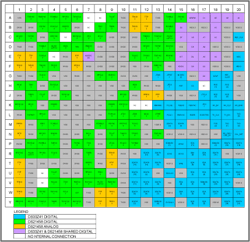
Tables 1, 2 and 3 and Figure 1 can help achieve netlist adjustments. Table 1 lists the external package pins of all DS33R41 connected only to the DS33Z41 die, Table 2 lists the external package pins of the DS33R41 connected only to the DS21458 die, and Table 3 lists the DS33Z41 and DS21458 die The external package pins of the connected DS33R41. For easy reference, Figure 1 rearranges the same content.
The DS33R41 engineering evaluation board designed by Cadence® Concept software uses a reduced netlist format to verify PWB netlist adjustments and JTAG boundary scan testing. Depending on the type of netlist and the capabilities of the designer, this process can be completed in about 30 to 60 minutes. Most of the editing of netlist files can be done by a text editor, but depending on the type of netlist, it can also be edited by Microsoft® Excel. Excel can adjust rows based on column data. After finishing editing, we must pay attention to some details. Irregular data such as file header and tail information must be retained, and the netlist must also be saved in the original format.
The following is a list of steps to complete this process: Use a text editor to open the netlist file and group the network nodes connected to the DS33R41 reference number into the same group. For example, the reference number of the DS33R41 package on the DS33R41 engineering evaluation board is U01; the nodes that are grouped in the first step are connected to the DS33Z41, to the DS21458, and to both. Use Figure 1, Figure 2 and Figure 3 and Table 1 to complete this work; Change the node reference number of all DS33Z41 from U01 to U01_D1 (device 1 representing U01 reference number), this step assumes that the reference number of DS33R41 is U01, If the reference number is not U01, you can change U01_D1 accordingly; change all DS12458 node reference numbers from U01 to U01_D2 (device 2 representing U01 reference number), this step assumes that the reference number of DS33R41 is U01, if the reference number is not U01, You can change U01_D2 accordingly; copy 22 common nodes, so in fact each common node has two, divide them into the above two groups; change the node reference number assigned to the first group in step 5 from U01 U01_D1, this step assumes that the reference number of DS33R41 is U01, if the reference number is not U01, you can change U01_D1 accordingly; change the node reference number assigned to the second group in step 5 from U01 to U01_D2, this step assumes the reference of DS33R41 The number is U01. If the reference number is not U01, you can change U01_D1 accordingly; save the newly created netlist. The newly created PCB netlist file actually contains two examples of the physical device DS33R41. The first example describes the pin connection related to the DS33Z41 part; the second example describes the pin connection related to the DS21458 part. This new netlist and two DS33R41 BSDL files and any corresponding test vectors can be loaded into any JTAG test software.
Although the methods described in this document have been tested and verified to work properly, other netlist formats may have some unknown characteristics. If you need additional assistance during the JTAG boundary scan test, please use the contact information below.
Table 1. DS33Z41 die device pins
Table 2. Device pins of the DS21458 die
Table 3. Common device pins for DS33Z41 and DS21458 die
Detailed pictures (PDF, kB)
Overview In the hardware manufacturing of telecommunication systems, one of the most basic tasks is to check for any production defects that may be contained in the system. Among the many hardware testing methods, one of the most commonly used methods is to use the Joint Test Action Group (JTAG) boundary scan method. The boundary scan test method will make some minor changes to the hardware before production, so hardware verification can be performed after production. In the design process, all integrated circuits (ICs) that support JTAG are connected in series in a daisy chain through the JTAG test interface, and verification is completed by a special JTAG test system connected to the test interface. The JTAG test system uses a printed circuit board ( PWB) Netlist, Boundary Scan Description Language (BSDL) files, and PWB connection test vectors verify point-to-point connections.
BSDL testing is simple. However, for multi-chip module devices, such as the inverse multiplexed Ethernet mapper DS33R41 with T1 / E1 / J1 transceivers, there is no way to include them in the BSDL file because they contain multiple die dies in one package Describe these devices correctly, but you can overcome this shortcoming by making minor changes to the PWB netlist and using two BSDL files to describe the device package.
Adjusting the netlist of the printed circuit board Before the JTAG boundary scan test, the part of the PWB netlist used to describe the external connection of the DS33R41 package must be split and adjusted to the connection of the internal DS33Z41 die and the DS21458 die. After completing this step, the netlist of the DS33R41 package will be defined by two independent reference numbers, which allow two different BDSL files to characterize the connection of the DS33Z41 and DS21458 inside the DS33R41 package, respectively.
Tables 1, 2 and 3 and Figure 1 can help achieve netlist adjustments. Table 1 lists the external package pins of all DS33R41 connected only to the DS33Z41 die, Table 2 lists the external package pins of the DS33R41 connected only to the DS21458 die, and Table 3 lists the DS33Z41 and DS21458 die The external package pins of the connected DS33R41. For easy reference, Figure 1 rearranges the same content.
The DS33R41 engineering evaluation board designed by Cadence® Concept software uses a reduced netlist format to verify PWB netlist adjustments and JTAG boundary scan testing. Depending on the type of netlist and the capabilities of the designer, this process can be completed in about 30 to 60 minutes. Most of the editing of netlist files can be done by a text editor, but depending on the type of netlist, it can also be edited by Microsoft® Excel. Excel can adjust rows based on column data. After finishing editing, we must pay attention to some details. Irregular data such as file header and tail information must be retained, and the netlist must also be saved in the original format.
The following is a list of steps to complete this process: Use a text editor to open the netlist file and group the network nodes connected to the DS33R41 reference number into the same group. For example, the reference number of the DS33R41 package on the DS33R41 engineering evaluation board is U01; the nodes that are grouped in the first step are connected to the DS33Z41, to the DS21458, and to both. Use Figure 1, Figure 2 and Figure 3 and Table 1 to complete this work; Change the node reference number of all DS33Z41 from U01 to U01_D1 (device 1 representing U01 reference number), this step assumes that the reference number of DS33R41 is U01, If the reference number is not U01, you can change U01_D1 accordingly; change all DS12458 node reference numbers from U01 to U01_D2 (device 2 representing U01 reference number), this step assumes that the reference number of DS33R41 is U01, if the reference number is not U01, You can change U01_D2 accordingly; copy 22 common nodes, so in fact each common node has two, divide them into the above two groups; change the node reference number assigned to the first group in step 5 from U01 U01_D1, this step assumes that the reference number of DS33R41 is U01, if the reference number is not U01, you can change U01_D1 accordingly; change the node reference number assigned to the second group in step 5 from U01 to U01_D2, this step assumes the reference of DS33R41 The number is U01. If the reference number is not U01, you can change U01_D1 accordingly; save the newly created netlist. The newly created PCB netlist file actually contains two examples of the physical device DS33R41. The first example describes the pin connection related to the DS33Z41 part; the second example describes the pin connection related to the DS21458 part. This new netlist and two DS33R41 BSDL files and any corresponding test vectors can be loaded into any JTAG test software.
Although the methods described in this document have been tested and verified to work properly, other netlist formats may have some unknown characteristics. If you need additional assistance during the JTAG boundary scan test, please use the contact information below.
Table 1. DS33Z41 die device pins
| Pin | DescripTIon | Pin | DescripTIon | Pin | DescripTIon | ||
| A1 | VSS | J18 | RXD [2] | P13 | VSS | ||
| B16 | VDD3.3 | J19 | RXD [0] | P14 | SDMASK [1] | ||
| B17 | VDD3.3 | J20 | VSS | P15 | SRAS | ||
| B19 | VDD3.3 | K3 | VSS | P16 | SDA [11] | ||
| B20 | VDD3.3 | K5 | VSS | P17 | VDD1.8 | ||
| C19 | VDD3.3 | K6 | VSS | P18 | SDMASK [2] | ||
| C20 | REF_CLK | K7 | VSS | P19 | SDATA [18] | ||
| D10 | VDD3.3 | K8 | VSS | P20 | SDATA [19] | ||
| D15 | VSS | K13 | RMIIMIIS | R11 | VSS | ||
| D18 | VDD3.3 | K14 | TCLKE | R12 | SDATA [12] | ||
| D19 | VDD3.3 | K15 | TSERO | R13 | SDATA [6] | ||
| D20 | VDD3.3 | K16 | TBSYNC | R14 | SCAS | ||
| E19 | VDD3.3 | K17 | JTDI1 | R15 | SDCS | ||
| E20 | MDC | K18 | RX_DV | R16 | SBA [0] | ||
| F11 | VSS | K19 | RX_CLK | R17 | SDA [10] | ||
| F14 | VSS | K20 | RX_ERR | R18 | SDATA [31] | ||
| F18 | VDD3.3 | L4 | VSS | R19 | VSS | ||
| F19 | VDD3.3 | L5 | VSS | R20 | VDD1.8 | ||
| F20 | MDIO | L6 | VSS | T11 | SDATA [13] | ||
| G4 | VSS | L7 | VSS | T12 | SDATA [14] | ||
| G5 | VSS | L8 | VSS | T13 | SDATA [5] | ||
| G7 | VSS | L14 | RCLKI | T14 | VDD1.8 | ||
| G12 | VSS | L15 | RBSYNC | T15 | SWE | ||
| G13 | JTMS1 | L16 | RSERI | T16 | SDA [8] | ||
| G14 | JTRST1 | L17 | DCEDTES | T17 | SDA [0] | ||
| G15 | MODEC [1] | L18 | TX_CLK | T18 | SDATA [16] | ||
| G16 | VDD3.3 | L19 | TX_EN | T19 | SDATA [27] | ||
| G18 | QOVF | L20 | TXD [0] | T20 | SDATA [26] | ||
| G19 | REF_CLKO | M5 | VSS | U11 | SDATA [15] | ||
| G20 | VSS | M6 | VSS | U12 | SDATA [4] | ||
| H5 | VSS | M7 | VSS | U13 | VSS | ||
| H6 | VSS | M12 | VSS | U14 | SDCLKO | ||
| H7 | VSS | M13 | VDD1.8 | U15 | VSS | ||
| H8 | VSS | M14 | SDATA [3] | U16 | SDA [1] | ||
| H9 | VSS | M15 | SDATA [1] | U17 | SDA [4] | ||
| H10 | VSS | M16 | VSS | U18 | SDATA [29] | ||
| H14 | JTDO1 | M17 | VDD1.8 | U19 | SDATA [25] | ||
| H15 | RST | M18 | TXD [2] | U20 | SDATA [24] | ||
| H16 | CS | M19 | TXD [1] | V11 | SDATA [11] | ||
| H18 | RXD [1] | M20 | TXD [3] | V12 | SDATA [10] | ||
| H19 | RXD [3] | N12 | VSS | V13 | SDATA [8] | ||
| H20 | VSS | N14 | VDD1.8 | V14 | VSS | ||
| J6 | VSS | N15 | VDD1.8 | V15 | SDA [9] | ||
| J7 | VSS | N16 | VDD1.8 | V16 | SDA [7] | ||
| J8 | VSS | N17 | VDD1.8 | V17 | SDMASK [3] | ||
| J9 | VSS | N18 | VSS | V18 | SDATA [30] | ||
| J15 | VSS | N19 | RX_CRS / CRS_DV | V19 | SDATA [22] | ||
| J16 | VDD1.8 | N20 | COL_DET | V20 | VDD1.8 | ||
| J17 | JTCLK1 | P12 | VSS | W11 | SDATA [0] | ||
| W12 | SDATA [9] | W19 | SDATA [20] | T16 | SDA [6] | ||
| W13 | SDATA [7] | W20 | SDATA [23] | Y17 | SDA [2] | ||
| W14 | VDD1.8 | Y11 | SDATA [2] | Y18 | VDD1.8 | ||
| W15 | SBA [1] | Y12 | VSS | Y19 | SDATA [28] | ||
| W16 | SDA [5] | Y13 | SDMASK [0] | Y20 | SDATA [21] | ||
| W17 | SDA [3] | Y14 | SYSCLKI | ||||
| W18 | SDATA [17] | Y15 | VDD1.8 |
Table 2. Device pins of the DS21458 die
| Pin | DescripTIon | Pin | Description | Pin | Description | ||
| A2 | TSSYNC3 | D3 | TCHBLK3 | G9 | RNEGO2 | ||
| A3 | RMSYNC3 | D4 | RLOS / LOTC3 | G10 | DVSS | ||
| A4 | RCHBLK3 | D5 | RSIG3 | G11 | DVSS | ||
| A5 | RPOSO3 | D6 | TPD | G17 | D0 | ||
| A6 | TSYSCLK3 | D7 | RNEGO3 | H1 | RCLK3 | ||
| A9 | TCLK2 | D8 | DVDD | H2 | TSIG3 | ||
| A10 | TVDD | D9 | DVDD | H3 | DVSS | ||
| A11 | TRING2 | D11 | DVDD | H4 | TSYSCLK1 | ||
| A12 | TTIP2 | D12 | RCLKO2 | H11 | RSIG2 | ||
| A13 | TVSS | D13 | TSYNC2 | H12 | RVSS | ||
| A14 | TCHBLK2 | D14 | RCHCLK2 | H13 | RVSS | ||
| A15 | RSYNC2 | E1 | TTIP3 | J1 | DVSS | ||
| B1 | DVSS | E2 | TTIP3 | J2 | TSERI3 | ||
| B2 | DVSS | E3 | TCHCLK3 | J3 | TCLKT3 | ||
| B3 | RSYNC3 | E5 | RVSS | J4 | DVDD | ||
| B4 | RCHCLK3 | E6 | RTIP3 | J5 | TSYSCLK2 | ||
| B5 | RSERO3 | E8 | DVDD | J10 | RPOSO2 | ||
| B6 | DVDD | E9 | DVDD | J11 | RVSS | ||
| B8 | TSIG2 | E10 | DVDD | J12 | RRING2 | ||
| B9 | TSERI2 | E11 | TCLKO2 | J13 | RTIP2 | ||
| B10 | TVDD | E12 | TPOSO2 | J14 | RVDD | ||
| B11 | TRING2 | E13 | TSSYNC2 | K1 | RSYSCLK1 | ||
| B12 | TTIP2 | E14 | RFSYNC2 | K2 | MCLK1 | ||
| B13 | TVSS | F1 | TRING3 | K4 | RSERO1 | ||
| B14 | RCHBLK2 | F2 | TRING3 | K9 | RSERO2 | ||
| C1 | RCLKO3 | F3 | TNEGO3 | K10 | RSYSCLK2 | ||
| C2 | TSYNC3 | F4 | TPOSO3 | L1 | RVSS | ||
| C3 | DVSS | F5 | RVSS | L2 | TRTRST | ||
| C4 | RFSYNC3 | F6 | RRING3 | L3 | BPCLK1 | ||
| C6 | RSYSCLK3 | F7 | RVDD | L9 | TCHCLK4 | ||
| C7 | JTDI2 | F8 | DVDD | L10 | JTDO2 | ||
| C8 | RCLK2 | F9 | DVDD | L11 | JTMS2 | ||
| C9 | DVDD | F10 | DVDD | L12 | MCLK2 | ||
| C10 | DVDD | F12 | DVSS | L13 | JTRST2 | ||
| C11 | DVDD | F13 | RMSYNC2 | M1 | RRING1 | ||
| C12 | TNEGO2 | G1 | TVDD | M2 | RVSS | ||
| C13 | TCHCLK2 | G2 | DVDD | M3 | RSIG1 | ||
| C14 | RLOS / LOTC2 | G3 | TCLKO3 | M4 | TCHBLK1 | ||
| D1 | TVSS | G6 | RVSS | M8 | RCHBLK4 | ||
| D2 | TVSS | G8 | BPCLK2 | M9 | RSYNC4 | ||
| M10 | RFSYNC4 | R5 | DVSS | V6 | RNEGO4 | ||
| M11 | TCLKO4 | R6 | DVSS | V7 | RCHCLK4 | ||
| N1 | RTIP1 | R7 | TSERI4 | V8 | RLOS / LOTC4 | ||
| N2 | RVSS | R8 | RVDD | V9 | RMSYNC4 | ||
| N3 | RPOSO1 | R9 | RRING4 | V10 | DVSS | ||
| N4 | RNEGO1 | R10 | RVSS | W1 | TRING1 | ||
| N5 | DVSS | T1 | TTIP1 | W2 | TVDD | ||
| N6 | DVSS | T2 | TVSS | W3 | TSYNC1 | ||
| N7 | RCLK4 | T3 | DVSS | W4 | TSSYNC1 | ||
| N8 | DVSS | T4 | DVSS | W5 | RCLK1 | ||
| N9 | TCLKT4 | T5 | DVSS | W6 | CST | ||
| N10 | TNEGO4 | T6 | DVSS | W7 | TVSS | ||
| N11 | TPOSO4 | T7 | RSERO4 | W8 | TTIP4 | ||
| N13 | TSSYNC4 | T8 | RVSS | W9 | TRING4 | ||
| P1 | RVDD | T9 | RTOP4 | W10 | TVDD | ||
| P2 | RCHCLK1 | T10 | RVSS | Y1 | RMSYNC1 | ||
| P3 | RCHBLK1 | U1 | TTIP1 | Y2 | RSYNC1 | ||
| P4 | TNEGO1 | U2 | TVSS | Y3 | TCHCLK1 | ||
| P5 | DVSS | U4 | TCLKT1 | Y4 | TSERI1 | ||
| P6 | TSYNC4 | U5 | DVSS | Y5 | TSYSCLK4 | ||
| P7 | TSIG4 | U6 | DVSS | Y6 | RSYSCLK4 | ||
| P8 | DVSS | U7 | RPOSO4 | Y7 | TVSS | ||
| P9 | JTCLK2 | U8 | RSIG4 | Y8 | TTIP4 | ||
| P10 | RCLKO4 | U9 | DVSS | Y9 | TRING4 | ||
| P11 | TCHBLK4 | U10 | DVSS | Y10 | TVDD | ||
| R1 | RFSYNC1 | V1 | TRING1 | ||||
| R2 | RLOS / LOTC1 | V2 | TVDD | ||||
| R3 | TPOSO1 | V4 | RCLKO1 | ||||
| R4 | TCLKO1 | V5 | TSIG1 |
Table 3. Common device pins for DS33Z41 and DS21458 die
| Pin | Description | Pin | Description | Pin | Description | ||
| A16 | WR / RW | C16 | A9 | E17 | A6 | ||
| A17 | D1 | C17 | A7 | E18 | A4 | ||
| A18 | A5 | C18 | A2 | F15 | RD / DS | ||
| A19 | A0 | D16 | D5 | F16 | D3 | ||
| A20 | A1 | D17 | A8 | F17 | D2 | ||
| B15 | D6 | E7 | MODEC [0] | G17 | D0 | ||
| B18 | A3 | E15 | INT | ||||
| C15 | D7 | E16 | D4 |
Detailed pictures (PDF, kB)
RAM/RFM Middle Frequency Water Cooled Capacitors
RAM/RFM Middle frequency water cooled capacitors
Water Cooled Capacitors,Medium Frequency Capacitor,Intermediate Frequency Capacitors
YANGZHOU POSITIONING TECH CO., LTD. , https://www.pst-thyristor.com