This article gives you a brief introduction to the TLV3501 comparator-AC-coupled single-supply comparator design, and hopes to guide you in designing a single-supply comparator.
Sometimes a single-supply comparator is required to detect sine or square waves using AC coupling. This single supply comparator is often required due to the ground potential difference between the two modules. As long as AC coupling is involved in a single-supply circuit, a negative voltage needs to be considered. Excessive negative voltage on the comparator can cause the comparator to trigger incorrectly or get stuck at an unpredictable level. In order to achieve a reliable operating point, suitable high conduction filtering and DC offset are required. This design will show how to ac-couple a wide range of input signal levels and frequencies into a high speed comparator to generate a robust, accurate and accurate clock signal.

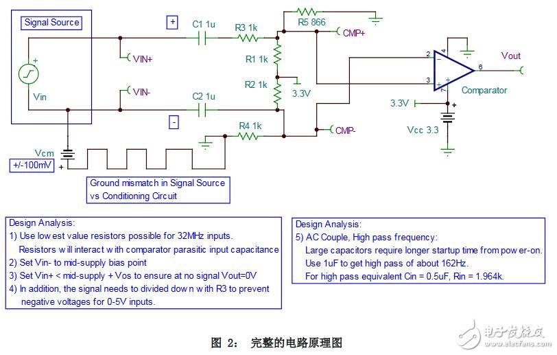
AC-coupled single-supplier comparator circuit diagram
Design summary
The design requirements are as follows:
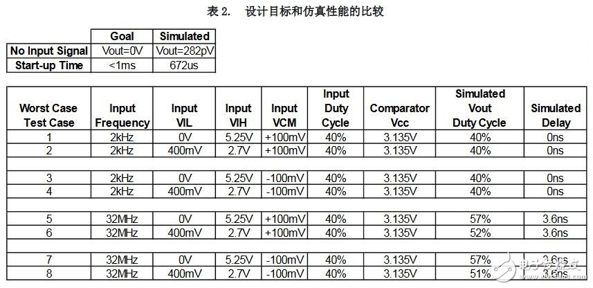
• No input signal -> Comparator output = 0V
• Startup time is less than 1ms
• Power supply voltage: 3.3V, +5% (3.135V to 3.465V)
• Input source provides:
• Vcc = 3.3V, +5% (3.135V to 3.465V)
• Vcc = 5V, +5%, (4.75V to 5.25V)
• Input signal level:
•VIL = GND+400mV @ Isink = 2mA
• VIH = Vcc-400mV @ Isource = 2mA
• Common mode range: +100mV
• Transmission delay: <5ns
• Change in duty cycle from input to output <10%
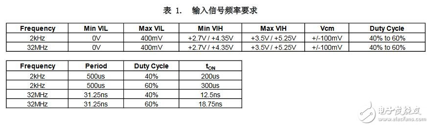
• Frequency requirements – see Table 1
TLV3501 comparator circuit: AC-coupled single-supply comparator,
The specific operation principle is as follows:
The “AC-Coupled Single-Supply Comparator†circuit design provides a way to neglect the indirect difference of the module and provides a wide range of frequencies and amplitudes into a high-speed comparator for a robust, accurate and accurate clock signal. Please refer to Figure 2. C1 and C2 provide AC coupling of the input signal Vin. R2 and R4 provide a DC offset for the CMP-medium supply. R1 and R5 provide CMP + a DC offset of approximately 100mV less than half the supply voltage. For the absence of an input signal, the DC offset difference between CMP- and CMP+ ensures that Vout is the comparator output low (near zero volts). The DC offset on each input is used to offset the negative voltages present at these inputs. These negative voltages are caused by the AC coupling of Vin. R3 divides the ac-coupled input signal by a magnitude that is less than the magnitude of the common-mode voltage of the comparator used. These input divider resistors are combined with the comparator input capacitor to form an input low-pass filter that attenuates the ac-coupled signal into the comparator. For this reason, in practical applications, it is necessary to keep the value of the resistance as low as possible. The high turn-on cutoff frequency of the input signal regulation can be thought of as a simple CR high pass with C = C1||C2 and R = 1.964k (through the range resistors, R1, R2, R3, R4, R5 are connected to CMP+ and CMP - The equivalent input resistance visible on the ends of C1 and C2).
For more TLV3501 comparator-AC-coupled single-supply comparator design, please refer to the following TI official website link address:
Http://
UPS-Charged Pure Sine Wave Inverter
Saintish inverter charger power ranges from 500W to 4000W. and DC voltage available in 12V, 24V or 48V.
It works as like UPS, when the public main power is available, the Inverter with charger will charge battery, when the main power disconnected, the inverter stop charging the battery immediately and transfer power from DC to AC, supplying the loads. All goes so fast the loads keep working without any problem.
Ups-Charged Pure Sine Wave Inverter, Inverter With Charger, Inverter Charger 2000W
Hangzhou Saintish Technology Co.,Ltd. , https://www.saintishtech.com