Historically, the development cycle of defense and civilian radar infrastructure has been long and requires a lot of time, innovation and capital investment. Defensive applications have always been a major force driving the development of radar infrastructure, but they often increase the total system cost while greatly improving the performance of the harvesting radar. These factors have contributed to the transition from traditional mechanically controlled radar structures to active electronically scanned arrays (AESAs, or active antenna arrays) that utilize advanced multi-beam capabilities to support the enormous benefits of time and space accuracy. AESA's versatility is equally compelling, and its new agility allows for the integration of completely different radar systems on a single platform (see Figure 1).
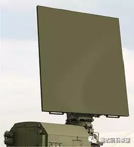
Figure 1 Active phased array structure supports electronic beam steering and multiple radars combined into a single system
These operational characteristics of AESA determine that this technology will replace traditional defense radar systems, and AESA devices have been well used in this field. With ground, sea and air deployment capabilities, AESA technology greatly enhances the network of sensors and enhances the situational awareness of modern battlefields. Applied to civil radar architecture, AESA has the potential to deeply influence citizens' personal safety and public safety. A single multi-functional AESA radar network can significantly improve the level of air traffic control while providing a significant increase in air traffic control capabilities, bringing direct economic benefits to the country and supporting national defense capabilities. Using AESA technology, meteorologists can better predict and evaluate some strong storms to save lives. AESA sensors also support the ability of unmanned and unmanned vehicles to integrate into mainstream society. This will fundamentally change transportation and commerce, leading to social change.
However, in order to achieve a successful transfer of AESA from defense applications to civilian and commercial applications, there are still some technical and economic challenges that need to be addressed. Continuing to rely on traditional RF devices and bulky assembly techniques, one of the results is hindering the important applications of AESA. In order to see the direction of this research, it is useful to clarify its origin and current development roadmap.
1 R&D roadmap
The next generation of active antenna technology dates back to project research in the 1960s. With the maturity of GaAs monolithic microwave integrated circuit (MMIC) technology in the 1980s, the development speed of AESA has also been accelerated. The Defense Advanced Research Projects Agency (DARAP) has partnered with MACOM and other technology companies to conduct microwave/millimeter wave monolithic microwave integrated circuit projects and microwave analog front end technology (MAFET) projects. These research projects have led to the advancement of advanced hybrid semiconductor technology from laboratory research to commercial manufacturing of RF devices, and the industry's first few watts of MMIC. The further development of these semiconductor and packaging technologies has led to the application of the first batch of RF modules and devices in mainstream printed circuit board (PCB) technology and surface assembly technology. The goal of these research activities after the DARPA project was to develop hybrid semiconductors with higher output power, higher efficiency and higher operating frequencies. Gallium nitride (GaN) technology has become a development and investment focus of AESA due to its high operating frequency (to 500 GHz), revenue, consistency and reliability.
DARPA's Business Time-Scale Array (ACT) program began in 2014 to leverage best practices from the commercial space to shorten the development and manufacturing cycles of next-generation radar, electronic warfare (EW) and communications systems. The ultimate goal is to implement digital interconnected phased array standard components, thereby building larger systems without the need for a complete redesign for each new application. The implementation of radar systems in this way is expected to shorten market time and costs, both of which are necessary for AESA to obtain mainstream applications for both civil and commercial applications.
2 slat array and tile array comparison
The cost and viability of AESA depends on the cost of its electronics and how these devices are built into the array. There are many factors that affect the cost of the final system, including the receiving/transmitting (T/R) module, RF boards, and cables.
The T/R module occupies approximately half of the cost of the radar phased array, and its own cost is determined by the MMIC type, package method, and module substrate. The traditional T/R module used in radar uses ceramic material as the substrate, and the manufacturing process adopts the "chip thin wire" method. In chip thin wire assembly, MMIC chips and other ICs require additional sanding work. This adds considerable expense compared to plastic sealed MMICs in commercial systems. Multilayer RF boards and cables in phased array designs account for almost all of the remaining cost (assembly, test, and fabric structures account for approximately 10% of total cost). As with the T/R module, the basic architecture of the array design adds more cost.
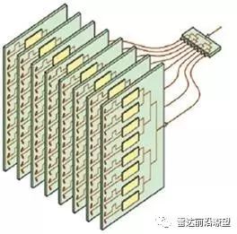
Figure 2 slat array
Here is an example of a conventional method of constructing a large phased array, known as a slat array structure, which has a number of slats perpendicular to the front (see Figure 2). Slat arrays have many advantages: they provide a large surface area for connecting T/R modules and supporting electronics. In addition, the thermal load of such a high power amplifier can be expanded in a large space, that is, the product of the aperture area and the thickness of the slab. The main disadvantage is that it requires a large number of RF boards and cables to transmit RF, DC, and control signals by installing and removing slats for array operation. This also increases the design cost.
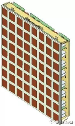
Figure 3 Tile Array
Another method is a tile structure, i.e., the array consists of a layered structure parallel to the front surface, which overcomes these drawbacks by employing a more compact structure (see Figure 3). The antenna unit and the RF beamformer are integrated on a single multi-layer RF board, and the T/R module is mounted directly on the back of the board. The advantage of this approach is that it significantly reduces the area of ​​the RF board and significantly reduces the number of connections and cables. The T/R module is designed to take advantage of high-volume commercial microwave packaging and manufacturing technology to further reduce costs. The T/R module MMIC of this architecture is packaged in an industry standard quad flat no-lead (QFN) package where the QFN package is soldered directly to an inexpensive PCB and the PCB is soldered directly to the back of the tile. The pure metal pads arranged on the edge of the printed circuit board are responsible for the RF and DC interconnection between the T/R module and the back of the tile.
By comparing the cell area relative to the transmit power and cell cost of the slab and tile array structure, it can be seen that at high power and low power output, the tile array can be reduced by more than five times.
3 multi-function radar
MACOM worked with the Massachusetts Institute of Technology (MIT) Lincoln Laboratory to optimize the structure of the tile array and validated the cost-effectiveness of using commercially available manufacturing processes. The multi-functional phased array radar (MPAR) project jointly developed by MACOM/Lincoln Labs is sponsored by the Federal Aviation Administration (FAA) and the National Oceanic and Atmospheric Administration (NOAA) and is designed for the next generation of civilian radars. It will be eight A separate traditional radar function is integrated into a multi-function platform. The first generation of MPARs (see Figure 4) uses scalable planar array (SSAR) tile arrays to detect and track meteorological conditions, aircraft and air targets.
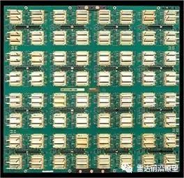
Figure 4 SPAR tile samples jointly developed by MACOM and Lincoln Laboratory
Although most conventional radar systems use mechanical rotation and tilt the radar's parabolic antenna to scan different airspace, SPAR tile radar consists of hundreds to thousands of T/Rs in a fixed planar array (airspace electronic scan). Unit composition. As shown in Figure 5, the MPAR's SPAR tile consists of a front-hole printed circuit board (APCB) containing radiating elements, transmit and receive beamforming networks, power and logic distribution. These T/R modules are surface mounted to the back of the APCB using standard industrial manufacturing processes. The second PCB, the backplane, contains DC power, a general purpose processor, and advanced logic. It combines with APCB to form a SPAR tile. The two PCBs are connected by low-cost, high-performance connectors and secured together using a simple mechanical structure to form a complete array of assembly structures.
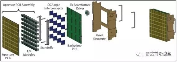
Figure 5 SPAR tile structure
The first deployed MPAR prototype is undergoing weather observation verification at the National Severe Storm Laboratory (NSSL) in Oklahoma, USA. It also provides a basic platform for developing back-end structures and AESA data-driven weather modeling algorithms. When fully operational, the system helps to increase the accuracy of forecasts for severe weather such as hurricanes, supporting earlier major storm warnings and other benefits. For the FAA, the MPAR system can significantly improve air traffic warnings and homeland defense surveillance.
For nearly a decade, MACOM has been promoting SPAR tile technology research. From proof of concept to the deployment of the first prototype system in the actual end application environment, the technical readiness (TRL) and manufacturing readiness (MRL) of the SPAR tiles have been improved. Based on the successful development of the first prototype system, MACOM has launched the first stage SPAR tile scale manufacturing, providing more than 90 tiles for FAA/NOAA Advanced Technology Verification (ATD) for full system verification. This is the first time to ensure a step-by-step statistics of performance indicators in a meaningful end-to-end manufacturing process. MACOM has manufactured and tested more than 6,000 T/R modules, and the results are shown in Figure 6.
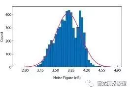
Figure 6 Noise figure distribution of the ATD T/R module. The histogram is close to a normal distribution with an average noise figure of 3.7 dB.
4 tile AESA opportunities
With the decline of traditional civilian radars used for air traffic control and weather monitoring, and the reduction of government spending, which has an impact on some important defense projects, the only way to develop a cost-effective new radar system is to combine innovative RF system architecture with commercial Manufacturing and processing are combined.
Tile AESA laid the foundation for the development of a new generation of high performance, agile radar systems. These radar systems are fast, cost-effective, and easy to upgrade and improve, and are widely used in defense, civil, and commercial applications. Design and assembly techniques for tile array MPARs can be used for both communication and sensing, supporting active antenna capabilities at a low price for a variety of commercial applications: airborne Internet, 5G technology, drone perception and Evasion and car radar.
Automotive Relay,Professional Four-Pin Relay,Micro Car Relay,Miniature Four-Pin Relay Relays
Ningbo Xingchuangzhi Electric Appliance Co.,Ltd. , https://www.xingchuangzhi.com