The basis of modern electronic products is semiconductor devices, so the performance of semiconductor devices determines the performance of the entire electronic product. The so-called semiconductor is the physical device whose electrical conductivity is between the conductor and the insulator. In the beginning, people were not interested in these substances, and later discovered the unique properties of semiconductors, with the irreplaceable advantages of conductors and insulators. The most common semiconductor device is a diode, and all other semiconductor devices are based on this.
Atomic structure and semiconductor devices
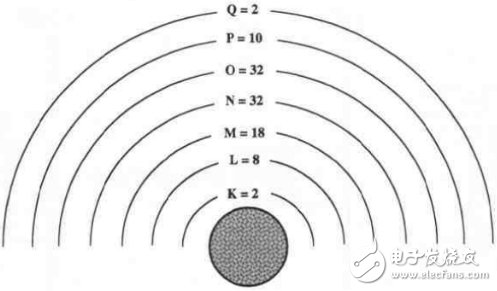
The conductor is electrically conductive because there are free electrons that are easy to move inside. The free electrons start to move under the action of the electric field. This motion is the current. The matter consists of atoms, each of which consists of a nucleus and free electrons orbiting it. It is generally divided into up to seven orbits from the outside to the inside, divided into K to Q, where there are two laws: First, the more the outer orbit, the smaller the electron energy, the easier it is to get out of orbit and become a free electron. The second is that when the electrons of the outermost track are 1 or the maximum number of electrons is decreased by 1, it is particularly easy to lose electrons or obtain electrons.

Figure 1: The electron shell of an atom
Electrons are generally negatively charged, and the orbital position of the lost electrons is called a hole and can be regarded as a positively charged particle. The substance carrying the current is called a carrier, and is generally a hole or a free electron. When a current flows, if a hole is more than a free electron, it is regarded as a carrier, and if there are many free electrons, a free electron is regarded as a carrier.
For semiconductors, their outer electrons are not so easy to lose, such as elemental silicon, which has four electrons on the outer layer, which are neither easy to lose nor easy to obtain, but can be doped with other elements to make it Free electrons or holes appear. Generally, if the hole is a majority carrier after the doping element, the P-type semiconductor is formed. After doping, free electrons appear as majority carriers or N-type semiconductors. When the two semiconductors are connected together, they have a very interesting characteristic - the current unidirectional flow, that is, the current can only flow from P to N, but not to reverse flow. However, if two P-type semiconductors and one N-type semiconductor (or two N-type semiconductors and one P-type semiconductor) are combined to form a triode, the triode has the following characteristics based on the nature of the diode:
1. Controllability of current flow. Normally, the triode cannot conduct electricity, but when an additional voltage switch is added, it can become a conductor and the flow direction can be controlled.
2, can play a role in the amplification of current. Under the action of the voltage switch, the number of carriers in the semiconductor increases and the current increases.
Under these two characteristics, if a periodic electrical signal is applied to the voltage switch, it will naturally amplify another periodic electrical signal, which will eventually become an electromagnetic wave after being released by the RF component. This is the basic principle of radar electromagnetic waves.
Wide band gap semiconductor
Large-scale integrated circuits of modern electronic devices are implanted on semiconductors. These semiconductors are called substrates. Through different doping, circuit components such as micro diodes, transistors, capacitors, and inductors can be effectively formed. A typical semiconductor substrate has a breakdown voltage, and once the voltage exceeds this limit, the diode is damaged. At the same time, it also corresponds to an electron drift rate, which is determined by the rate at which the free electrons of the material are separated from the original electron orbit and combined with the new electron orbit. The ease of detachment is called the forbidden band width, and the wider the band gap, the corresponding breakdown voltage. The larger the larger the output power of the semiconductor device, the faster the corresponding switching speed of the circuit, so that a higher frequency microwave device can be used.

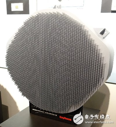
Figure 2: The AN/APG-73 radar used in the F-22 uses a microwave power device with a GaAs substrate to achieve high power and frequency.
Most of the semiconductor substrates used in electronic products are doped with silicon, boron and phosphorus. Due to the low technical difficulty and low cost, many electronic products for commercial and civilian use are still in use. However, these are obviously unusable when making military high-power microwave devices. Later, a GaAs (gallium arsenide) substrate was used, and its electron drift rate and breakdown voltage were more than 10 times higher than that of the silicon device. The phased array radar on the F-22 used the components of the substrate. The latest substrate materials surpass GaAs by an order of magnitude, which is GaN (gallium nitride) and SiC. In this respect, the United States and Japan are currently in the forefront. These two substrates have already reached the stage of engineering application, and China is currently only manufactured by the Chinese Academy of Sciences. Single crystal SiC came out, and it was not possible to carry out actual engineering mass production.
It can be said that in the future electronic system, whoever has the upper hand in wide-bandgap semiconductor devices, who can win in electronic warfare, China must attach great importance to this industry.
FUME EXTRA 1500PUFFS
Shenzhen Xcool Vapor Technology Co.,Ltd , http://www.xcoolvapor.com