The system block diagram is shown in Figure 1. It is mainly composed of AT89C52 MCU, XOR device, LCD 1602, power supply and so on.
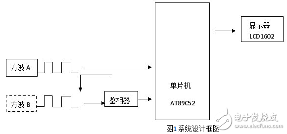
The timer/counter works in mode 1. Each time a timer 0 interrupt is generated, 65536 pulses are counted. The pulse at this time comes from the oscillator's 12-divided pulse, and its period is 1uS. According to the number of times the timer 0 interrupt is generated when the external interrupt 0 is generated, and the value X of the timer/counter 0 count register at this time, the period of the square wave to be tested can be obtained as: T=(65536*u+X)us The frequency of the square wave to be tested can be obtained by taking the reciprocal number, and two bits are reserved after the decimal point, so that the frequency precision is 0.1HZ.
Phase difference measurement principleThe ratio (duty ratio) of the pulse width t obtained by adding two square waves of different phase signals to the phase detector (ie, exclusive OR) and the period T of the square wave signal, that is, the phase difference between the two signals At this time, the phase difference

Among them, the measurement method of the pulse width is the same as the measurement method of the square wave period. The schematic of the phase difference measurement is as follows:

In this design, the P0 port (32~39 feet) is defined as the N1 function control port, which is connected to the corresponding function pin of N1. When the microcontroller is working normally, it needs a clock circuit and a reset circuit. In this design, the internal clock mode and the button level reset circuit are selected to form the minimum circuit of the microcontroller. As shown in Figure 4.
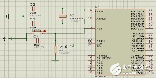
Figure 4 MCU minimum system
The overall circuit diagram of the frequency and phase diagram is shown in Figure 5:
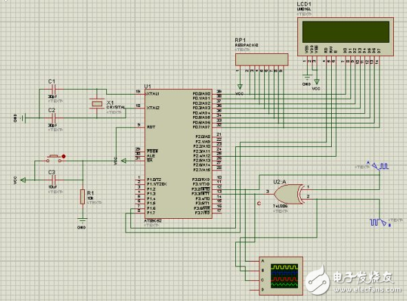
Figure 5 Overall circuit diagram of the frequency phase meter
Design scheme based on simple digital frequency meter of single chip microcomputer (2)In this paper, we use a frequency divider function of prescaler SAB6456A and high-speed digital divider 74HC390, combined with a new MSP430F449 microcontroller, to give a novel, fully automatic digital display measurement RF frequency design.
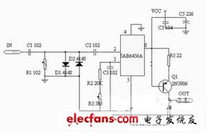
Figure 1 Signal front-end processing and frequency dividing circuit
Main device introductionMSP430F449 microcontroller
The MSP430F449 features a 16-bit RISC architecture with extensive on-chip peripherals and high-capacity on-chip working registers and memory for a high price/performance ratio. Its features include:
Ultra-low power consumption: capable of operating from 1.8V to 3.6V; with operating mode (AM) and 5 low power modes (LPM). In low power mode, the CPU can be awakened by interrupts with a response time of less than 6ps.
· Strong computing power: 16-bit RISC structure, rich addressing mode; 16 interrupt sources, can be arbitrarily nested; instruction cycle can reach 125ns under 8MHz clock drive; internal hardware multiplier and a large number of registers, And up to 64KB of Flash program space and 2KB of RAM, to ensure the storage of data and operations.
· Rich on-chip peripherals: including watchdog timer, basic timer, comparator, 16-bit timer (TA, TB), serial port 0, 1, liquid crystal display driver, 6 8-bit I/O ports, 12-bit ADC (maximum sampling rate 200kHz) and so on. A rich set of on-chip peripherals makes it easy to build a more complete system. In addition, the multi-channel arbitrary waveform generation function and interrupt control function of the counter are fully utilized to ensure the completion of some complicated timing control tasks.
· Convenient and efficient development environment: MSP430F449 is a Flash-type device. There is a debug interface and an electrically erasable flash memory on the chip. You can download the program to the Flash first, and then run the software control program in the device, read by the JTAG interface. Take in-chip information for designers to debug. This method does not require an emulator and a programmer, and debugging is very convenient.
Prescaler SAB6456A
The SAB6456A is a prescaler designed for UHF/VHF. The internal MCpin is a frequency division control terminal, which can divide the frequency of the frequency range from 70MHz to 1GHz by 64/256. When the MC pin is open, it is divided by 64. When the MC pin is grounded, it is divided by 256. High sensitivity and strong harmonic suppression.
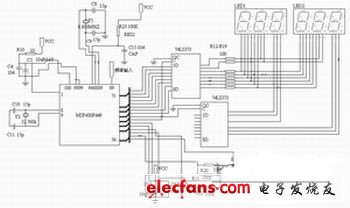
Figure 2 microcontroller peripheral circuit
working principleThe design is divided into two main parts: frequency division and counting. First, the input signal is clipped and divided by SAB6456A. ​​The 256-divided signal is divided by two 74HC390 high-speed crossovers. The analog signal becomes a low-frequency digital signal with a frequency below 10 kHz. Secondly, the sub-divided The signal after the frequency is directly connected to the MSP430F449 MCU, and the internal 16-bit timer A is used for timing and counting. The timer can be divided into several parts: the counter section, the capture/compare register, and the output unit. Among them, the counter has 4 working modes and 3 capture/compare registers. Using the continuous counting mode of the counter and the rising edge capture mode, the time of the N pulse signals is counted in the timer interrupt, and the frequency is obtained by dividing N.
hardware designFigure 1 shows the front-end processing and crossover design of the signal. The output signal is divided by two SN74HC390s. The SN74HC390 is a high-speed crossover device with a maximum frequency division of 50MHz. Each SN74HC390 can achieve a frequency division of 100. It adopts two series connection, which can realize the frequency division of the signal by 1000. The frequency of the digital signal after frequency division is lower, about 4 kHz or less, which can be directly counted by the single chip microcomputer.
Figure 2 shows the peripheral circuit of the microcontroller, including the reset circuit, the power supply circuit and the crystal oscillator necessary for the operation of the microcontroller. The crystal oscillator has 8MHz and 32.768kHz, 8MHz is used as the counter input clock source of timer A; 32.768kHz is used as the display frequency of the digital tube. 74LS373 is a D-type latch, 5V single-supply power supply, because the output current is large enough, it can also directly drive the common cathode LG3631AH digital tube.
software designConnect the divided output terminal OUT to the frequency input end of the MCU, and the program starts to delay for a period of time before the signal is stable. Open capture interrupt and timer A, count N pulses in timer A interrupt, get N pulses after measurement ends, then divide N to get the frequency of the pulse, multiply by the frequency division coefficient to get the actual frequency and display, after a short time Re-measure after delay, so cycle measurement and display.
When measuring the frequency, the LED display is turned off to ensure the accuracy. Therefore, for the lower frequency signal, the LED flashing occurs. The solution is to measure fewer pulses to reduce the average measurement time or reduce the delay.
Dynamic scanning display, the principle of dynamic scanning display is: P4 sends the scanning signal to each bit in turn, so that only one digital tube is strobed at each moment, and then P3 inputs the displayed font code to the bit to drive the The bit glyphs display glyphs. In this way, under the cooperation of the code segment sent by P3 and the bit segment sent by P4, each digital tube is alternately displayed with its respective glyph, and the display time of each bit is more than 1 ms, so that the human eye does not feel flicker.
The main measurement procedure is as follows:
Void frequency_measure(void)
{float tmp,tmp1;
Key_flag=0;//The button flag is cleared.
P1OUT|=BIT0;
Delay(1000); file://delay for a while and wait for the signal to stabilize
While(1)
{ IE2&=~0X80; file://off BT, off LED
Firstflag=1;//Start measuring the first pulse
TACTL|=TAIE; file://open capture
CCTL1|=CCIE;//Open TImer a
While (f_ok_flag==0);//waiting for the end of the measurement
F_ok_flag=0;
If (aa1"aa2)
Overflow=overflow-1;
Tmp=aa2-aa1;
Tmp1=40.0/(overflow*0.008191875+(tmp/8000000.0));
Result=tmp1*0.256;
IE2|=0X80; / / open BT, open LED
Yanshi (2, 2); / / can modify the parameters here, the larger the longer the delay, too small, the LED will be dark
CCTL1&=~CCIE;//Off capture
TACTL&=~TAIE;//Off TImer a
Return;
}
}
The flow chart is shown in Figure 3.
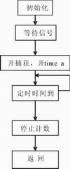
Figure 3 main program flow
ConclusionThe hardware and software given in this paper have been tested by practice, and the accuracy of the results measured by the measuring instrument is high. The measuring instrument is low in price and simple in structure, and is an economical frequency tester.
Design scheme based on simple digital frequency meter of single chip microcomputer (3)The digital frequency meter will measure the frequency by means of timing and counting, and dynamically display 6 digits using a 1602A LCD display. The measurement range is from 1 Hz to 10 kHz sine wave, square wave, triangle wave, and the time base width is 1 us, 10 us, 100 us, 1 ms. The automatic measurement function is realized by a single chip microcomputer.
The basic design principle is a measuring device that directly displays the frequency of the signal under test using a decimal number. It automatically measures the frequency of sine, square and triangle waves in a measurement cycle.
Design idea and frequency calculation of frequency measuring instrumentThe design of the frequency measuring instrument is mainly to divide the signal, measure the number of cycles of the known standard frequency signal in one or several measured signal periods, and then measure the frequency of the signal. The principle is as shown in Figure 1 on the right. Show.
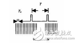
If the period of the signal to be measured is, the frequency division number m1, and the period of the frequency-divided signal is T, then: T=m1Tx. As can be seen from the figure: T=NTo
(Note: To is the period of the standard signal, so T is the period of the divided signal, then the frequency f of the signal to be measured can be calculated.)
Since the standard frequency of the single-chip system is relatively stable, but the error of the standard signal frequency of the system is usually small, and the quantization error of the system is less than 1, it can be known from the formula T=NTo that the error of the frequency measurement mainly depends on the value of N. Size, the larger the value of N, the smaller the error and the higher the accuracy of the measurement.
Basic design principleThe basic design principle is a measuring device that directly displays the frequency of the signal under test using a decimal number. It automatically measures the frequency of sine, square and triangle waves in a measurement cycle.
The so-called "frequency" is the number of times the periodic signal changes within a unit time (1 s). If the number of repeated changes N of the periodic signal is measured within a certain time interval T, the frequency can be expressed as f=N/T. The function of the pulse forming circuit is to change the signal to be measured into a pulse signal whose repetition frequency is equal to the frequency fx to be measured. The time reference signal generator provides a standard time pulse signal. If the period is 1 s, the output signal duration of the gate circuit is also exactly equal to 1 s. The gate circuit is controlled by a standard second signal. When the second signal comes, the gate is opened, and the measured pulse signal is sent to the counting decoding display circuit through the gate. At the end of the second signal, the gate is closed and the counter stops counting. Since the number of pulses N counted by the counter is the cumulative number in one second, the measured frequency fx = NHz.
Hardware structure design of digital frequency meter (low frequency)System hardware composition
The main component of the data acquisition system of this frequency meter is the single-chip AT89C51, which completes the functions of counting and displaying the frequency of the signal to be tested, and externally has a frequency divider, display and other devices. Can be divided into the following modules: amplification shaping module, second pulse generation module, shift analog conversion module, single-chip system, LCD display module. The relationship diagram of each module is shown in Figure 2:
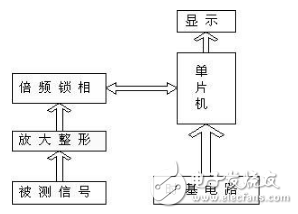
The general schematic of the system works as shown in Figure 3:
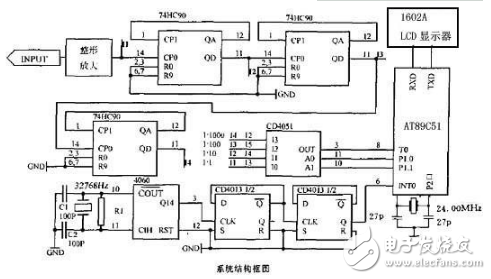
Figure 3 digital frequency meter system working principle diagram
Signal Conditioning and Amplification Shaping Module
The amplification shaping system includes an attenuator, a follower, an amplifier, and a Schmitt trigger. It forms a sinusoidal input signal Vx into a square wave Vo of the same frequency, and the measured signal with an excessive amplitude is divided and divided into a post-stage amplifier by a voltage divider to avoid waveform distortion. The emitter follower consisting of an operational amplifier acts as an impedance converter to increase the input impedance. The op amp of the non-inverting input has a magnification of (R1+R2)/R1. Changing the size of R1 can change the magnification. The shaping circuit of the system consists of a Schmitt trigger, and the shaped square wave is sent to the gate for counting.
Since the input signal amplitude is uncertain, it may be large or small, it is inconvenient to measure the input signal. If it is too large, the device may be burnt. If it is too small, the device may not be detected. Therefore, it is used in the design. The signal conditioning circuit performs impedance transformation, amplification limiting and shaping on the input waveform, and the signal conditioning part circuit realizes the circuit schematic diagram and parameters as shown in FIG. 4:

Time base signal generation principle:
This circuit adopts 32768HZ crystal oscillator, and uses CD4060 chip to obtain 2HZ signal (32768/214) after 14-stage frequency division. After passing CD4013 double D flip-flop, the square wave of 0.5HZ is obtained by dividing by two, that is, the second pulse signal is output. The microcontroller performs counting.
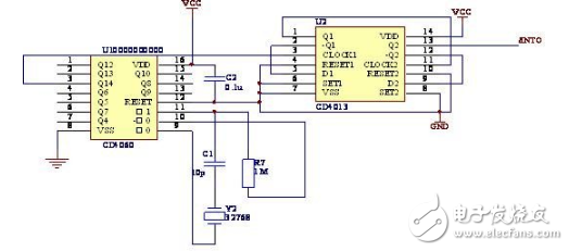
Figure seven second pulse generation circuit schematic
ShenZhen Antenk Electronics Co,Ltd , https://www.antenk.com