Low-power portable electronic products currently use lithium batteries and Boost (Buck) chips to power MCUs, Audio, and display devices. These products are typically powered by an adapter that is designed to pass the test and meet EMC standards when the charging section is in operation. In general, in order to improve the efficiency of the system, the lithium battery charging chip is based on the switching mode of operation, similar to a switching power supply. In addition, other switching power supply chips may work at the same time, and the devices are all switching modes, which improves the working efficiency. At the same time, the radiation problem has been introduced, which is also a common problem in the design process of electronic products. This article is based on a product design example (using the BQ24133 single-cell charging circuit and the LM3478 boost circuit) to analyze the radiation problems that have been encountered during the design process. Determine the source of the disturbance, find the coupling path, and finally give a solution to the problem for your reference.
This article refers to the address: http://
content
Portable audio product power system introduction
1.1 Background
In actual product development, EMI testing of portable products uses an adapter to charge the product, and other external devices need to be connected during testing. Let's take the development of an actual product as an example to illustrate the problems that should be paid attention to in the EMI design of such product design, and how to analyze the problem caused by the radiation emission exceeding the standard. And find a solution to the problem.
1.2 Audio product power supply circuit
Figure 1 below is a schematic diagram of the power section of an Audio product. This product has a charger chip BQ24133, which sets the maximum charging current of 2A in this application. There is a Boost chip LM3478, which boosts the battery voltage to 10V to power the Audio chip, with a full load current of 1A, and another Boost chip LM3478, which raises the battery voltage to 5V and charges the iPhone or iPad with a maximum current of 2A. The DC output line specification of the adapter is 1.5 meters, the power cord for charging the mobile phone is about 0.5 meters, and the entire PCB board area is about 12mm × 8mm. It is designed as a two-layer board.
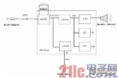
Figure 1: Audio power supply circuit diagram
2. Analysis of EMI problems
2.1 Generation of EMI problems
This type of portable product is required to pass the standard EN55022, Class B. The prototype of this product was tested in the radiation emission test (not connected to the mobile phone), and the radiation emission from 30M to 300M was seriously exceeded. It was around 200MHZ and exceeded 20DB.
2.2 Analysis of the reasons for the excessive emission of radiation:
First, we first analyze the causes of radiation overshoot. We know the three elements of EMC, disturbance sources, coupling paths and sensitive equipment. The device in the switching mode of this product is undoubtedly the source of disturbance, namely BQ24133 (switching frequency 1.6MHZ) and two LM3478 (switching frequency 400KHZ). Looking at the coupling path, the wavelength corresponding to the 30M to 300M frequency band is one meter to ten meters. If a certain wavelength of electromagnetic wave is to be transmitted, a transmitting antenna is needed. The necessary condition for the antenna is that the length is at least one-twentieth of the wavelength. When the antenna is an integer multiple of the half wavelength of the electromagnetic wave, the transmission power is the largest. The wire that satisfies the above conditions to become an antenna is just a few external wires, most likely the DC power and ground wires of the adapter. Analysis of the layout design, found that the product design, only used one place, the entire floor of the entire PCB is laid on a large area, and connected with the ground wire of the adapter, plus the charging wire of the mobile phone, forming a more than two meters Long ground wire. In addition, the BQ24133 charging circuit and the two LM3478 boost circuits are also large-area grounding, causing high-frequency interference to be directly coupled to the ground plane and emitted through the long ground.
3. Ways to solve the problem:
In response to the above analysis, a rectification was made. Because it is a portable audio device, there is no PE line, Y capacitor can not be used, and customers do not want to use common mode inductors to increase the cost, so the layout is mainly optimized. The following measures were taken:
3.1 Layout Notes:
1) Combine each power circuit, separate the analog ground from the digital ground, and do not cross each unit circuit. The digital ground and analog ground of the BQ24133 are separated and routed through a single point of 0 ohm resistor under the chip. In addition, the power of the BQ24133 is preferably split with the entire product, and connected at a single point.
2) Reduce the harmonic loop area. For the LM3478, as shown in the figure, when the MOS transistor is turned on, Cin, L and MOS form a loop to charge the inductor. See Cycle1 in Figure 2(a). When the MOS transistor is turned off, Cin, L, D, and Cout form another loop to discharge the inductor. See Cycle2 in Figure 2(b). For diode D, it alternates between forward conduction and reverse cutoff. Therefore, there is a high reverse recovery spike voltage. Snubber circuit is needed at both ends of the diode to suppress this spike voltage to avoid excessive total Mode noise. The operating frequency of these two loops is the switching frequency of the MOS, the harmonic component is large, and the area of ​​the harmonic loop should be minimized when laying the board. It is necessary to place the devices of the two power loops close to each other, and take a large copper-thick trace to reduce the loop impedance of the switching frequency harmonics.
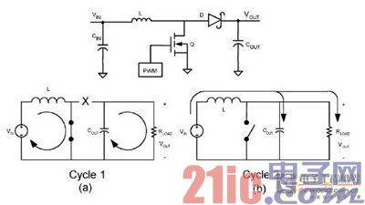
Figure 2: LM3478 working principle diagram
BQ24133 is essentially a Buck loop. There are similar problems. Please refer to Figure 3, BQ24133 working principle diagram, input capacitor C1, rectifier open, freewheeling switch off, rectifier inductor and load form a high frequency loop with high dI/dT. In addition, when the rectifier is turned off and the freewheeling tube is turned on, the inductor current flows through the freewheeling tube (the freewheeling tube operates in the continuous mode of the inductor current during heavy load), and the rectifier tube is turned on when the inductor current is not reduced to zero. This is the freewheeling tube is forced to add reverse voltage and cut off, resulting in a very high reverse recovery voltage spike (although synchronous rectification, due to the presence of dead zones, diode rectification in the dead time), which leads to comparison Large common mode noise, so a Snubber circuit is added to the SW to PGND to suppress the reverse spike of the freewheel. Therefore, the input filter capacitor C1, inductor L1 and output filter capacitor C2 should be placed as close as possible to the chip to reduce the high-frequency loop area. Power circuit traces should be routed with large copper strips to reduce harmonic impedance. It is best placed on the same layer of PCB. Snubber is placed close to the lower tube.
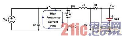
Figure 3: BQ24133 high frequency current loop diagram
In general, the input and output of the LM3478 and BQ24133 take a large copper bump, and the input capacitor and output capacitor are placed close to the power switch tube to minimize the area enclosed by the loop. Selecting a smaller ESR capacitor, due to cost reasons, the capacitance of these products is relatively poor, this project originally used electrolytic capacitors, it is recommended to add more ceramic capacitors in combination, so that good results at low cost. In this way, the harmonic circuit of the switching frequency of the input and output is as small as possible, the harmonic impedance is as small as possible, and the external radiation interference of the loop can be reduced.
3) As mentioned above, in the BQ24133's lower tube plus Snubber circuit (added between SW and PGND), the LM3478's freewheeling diode plus Snubber circuit. The Snubber circuit is placed close to the switch pin, widening the trace, and the high frequency harmonics are bypassed. First, you can pre-place a 2-3 ohm resistor with a capacitance of 500-1000 pF. In the radiation test, if the margin is insufficient or over-sized, increase the RC appropriately to absorb more high-frequency energy. If the margin is too large, reduce the value of RC to improve efficiency.
4) For the two-layer board, remove or reduce the GND copper under the trace between the power device and the power device such as the inductor and MOS. Reduce the distributed capacitance of the switch to GND to reduce common mode coupling.
3.2 Other considerations
3.2.1 Layout
In general, if possible, separate the power supply circuit from other circuits as much as possible. For example, place the power-type device on the left side of the PCB and leave the isolation tape properly with other circuits. The output lines and terminals should be as far away as possible from the switching tube, inductors and other devices. On circuits with large harmonics, pay attention to the PCB traces to avoid sharp angles, try to make obtuse angles or round corners.
3.2.2 Use of common mode inductors
For multi-cell batteries, the charging power is increased, and the battery output line is reduced as much as possible to prevent the battery line from becoming a radiating antenna. In addition, it is considered to appropriately increase the common mode inductance to suppress the common line interference of the battery line.
3.2.3 Test Considerations
It is recommended that the customer use the battery plus 1.5 m line as the input source during the radiation test to eliminate the interference caused by the Adapter. In addition, the Snubber parameter is adjusted during the test to achieve a balance between efficiency and EMI. The value of RC cannot be increased too much to avoid overheating of the IC. Therefore, when the noise of the interference source is relatively large, it is necessary to consider various measures at the same time to achieve the optimal effect.
4 Conclusion:
After the rectification, the layout was optimized and the radiation test was successfully passed. From this project, summarize some experiences. First, identify the source of disturbance and the transmit antenna, and increase the high-frequency harmonics of the Snubber circuit that absorbs the disturbance source. Secondly, judging the coupling path, the focus is on optimizing the layout so that the harmonics are bypassed by the capacitor bypass, reducing the high-frequency disturbance of the disturbance source to the coupling of the external long line. The essence of EMC design is how to deal with harmonics.
ZGAR AZ Vape Pods 5.0S
ZGAR electronic cigarette uses high-tech R&D, food grade disposable pod device and high-quality raw material. All package designs are Original IP. Our designer team is from Hong Kong. We have very high requirements for product quality, flavors taste and packaging design. The E-liquid is imported, materials are food grade, and assembly plant is medical-grade dust-free workshops.
From production to packaging, the whole system of tracking, efficient and orderly process, achieving daily efficient output. WEIKA pays attention to the details of each process control. The first class dust-free production workshop has passed the GMP food and drug production standard certification, ensuring quality and safety. We choose the products with a traceability system, which can not only effectively track and trace all kinds of data, but also ensure good product quality.
We offer best price, high quality Pods, Pods Touch Screen, Empty Pod System, Pod Vape, Disposable Pod device, E-cigar, Vape Pods to all over the world.
Much Better Vaping Experience!


ZGAR AZ Pods 5.0S Pods,ZGAR AZ Vape Pods 5.0S,ZGAR AZ Vape Pods 5.0S Pod System Vape,ZGAR AZ Vape Pods 5.0S Disposable Pod Vape Systems
Zgar International (M) SDN BHD , https://www.zgarette.com