PCB solderable surface coating (plating) coatings such as chemical Ni/Au (ENIG), electroless tin plating, electroless silver plating, electroless Ni/Pd/Au (ENEPIG) and organic solderability protectant (OSP) are not nano Graded surface coated (plated) materials with a surface coating thickness of 300 nm (0.3 um) or more. The surface coating of the newly developed Organo Metals OM (Organic Metals) is 50 nm, and more importantly, in the 50 nm thick OM surface coating layer, they are about 90% conductive polyester (ConducTIve Polymer). The material is composed of 10% metal Ag (actually Ag is only 4 nm thick), so it is superior to all current surface coating materials.
1 Overview
The organometallic OM is a special organic material, that is, it is a conductive polymer having metallic properties. It is an organometallic OM material having a particle size of 10 nm which is "synthesized" and "dispersed". Organometallic OM materials are very effective in preventing copper oxidation, which was established a few years ago. Surface coating applied to PCBs is very economical. At the same time, excellent solderability is achieved even after storage and thermal aging. Therefore, it is very advantageous to carry out surface coating (preparation) of the organometallic OM prior to immersion tin deposition. More prominently, OM is one of the Top-Quality surface coatings. This process can be widely used in the PCB industry and can be used in the manufacture of lead-free soldered electronic products.
In this technical process, an adsorption layer (Ad SO rb ed Laye r) of about 80 nm thick can be formed on the copper surface by the OM prepreg treatment, thereby causing selective formation of Cu+, thereby protecting the underlying Cu. At the same time, Cu+ acts as a catalyst to provide "electrons" for Sn2+, which deposits S n onto the Cu surface.
In the past 10 years, through the careful research and exploration of 0rmecons, the successful completion of the "organic nano metal" provides an excellent surface coating for the PCB. Three years ago, the market was offered as the first "nano surface coating" based on 0M. The 0M-based "nano-surface coating" not only has a high enough resistance to heat change (Di sc010 raTIon) but also is suitable for lead-free soldering conditions, and now a new generation of 0M-Ag complexed nano-surfaces The Composite Nanorfinish has been introduced and has shown better performance in terms of anti-aging, anti-change (return) and solderability.
2 process description and performance introduction
The following is the process of forming the nano surface coating layer of OM-Ag complex and its performance experiment.
2 .1 Process
The process begins with a special acid cleaner, which is specially micro-etched and then immersed in the panels for a short period of time (adjusted for 10 s) into the activation tank (0MN7100, 35°C/90 s). Rinsing and drying are completed. The processing flow is as follows:
Acid Cleaner - Rinsing - Micro Etching - Rinsing - Adjustment - OM Tank - Deionized Water Rinsing - Drying
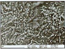
Structural studies (Morphology Inves TI 2a TIon) were performed on the plate samples by scanning electron microscopy (SEM) and electrostatic coulometric measurements (GCM). Figure 1 shows the scanning electron microscope image of the copper pad surface of the PCB after OM/A2 nano surface coating treatment. The SEM image shows that the 0M-Ag complex is at the interface of copper crystal, and most of the area (region ) is the surface of copper.

Figure 1 SEM image of PCB after OM/Ag nano surface coating treatment
2 .2 Coulometric Study (couIometric lnvestigation)
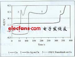
Electrochemical studies using GCM (Galvanostatic Coulomet: ric Measurement) showed that a 0M-based nano surface coating formed a novel complex, as shown in Figure 2. The potential (potential) of this novel complex is clearly distinguishable from the ordinary (simple) Ag on the Cu surface.

Figure 2 Gu, "potential-time" curve of immersion of Ag on Cu and OM/Ag on Cu
The relationship of the surface coating of the OM/Ag nanoparticle complex to copper is dependent on the immersion time, the situation of which is shown in FIG. The potential (pressure) size indicates that the copper surface will slowly decrease as the processing begins, with the highest coverage between 40s and 60s, while the copper-free coverage after 60s will slowly decrease and After 90 s detection (electrochemical can be seen) less than copper.
The excellent solderability results of the OM-based nano surface coating layer were confirmed by objective evaluation. A comparison between the widely used organic solderability protectant (OSP) and the OM-based nano surface coating is also carried out, mainly using solderability analysis and wetting balance to determine their wetting force. (Wetting Force). The test results show that the wetting force (1.0 mN) of the OM-based nano surface coating layer is almost twice that of the OSP secret coating layer (0.55 m).
Solder welding
An external objective analysis shows that lead-free solder soldering with BGA pads using 0M/Ag nanoscale surface coatings has a high quality solder structure. It is expected that welding using an OM/Ag nano-scale surface coating layer has long-term reliability.
3 conclusions
The OM/Ag nanoscale (particle size) complex can be used as a solderable surface coating (plating) layer for PCBs. It has a thinner thickness (50nm, only about 1/6 of the thinnest electroless silver plating) and can be used in lead-free soldering conditions. At the same time, the OM/Ag nano-scale solderable surface coating layer is anti-aging and anti-deformation (return) compared to the non-nano-scale conventional solderability surface coating (plating) layer (including the 0 SP coating layer, etc.). Better performance in terms of color and solderability.
Hongkong Onice Limited , https://www.osbvapepen.com