The PIC18FX455/X550 family of devices includes a full-speed and low-speed compatible USB Serial Interface Engine (SIE) that allows high-speed communication between any USB host and PIC microcontroller. The SIE can be connected directly to the USB using an internal transceiver or via an external transceiver. The internal 3.3V regulator can also be used as a power source for internal transceivers in 5V applications.
The USB module also includes some special hardware to improve its performance. Dual-port memory is provided in the device's data memory space (USB RAM) for direct memory access between the microcontroller and the SIE. In addition, a buffer descriptor is provided to allow the user to arbitrarily set the memory area in the USB RAM space for the endpoint to use. A parallel communication port is also provided to facilitate uninterrupted transmission of large amounts of data, such as transferring data isochronously to an external memory buffer.
USB status and control
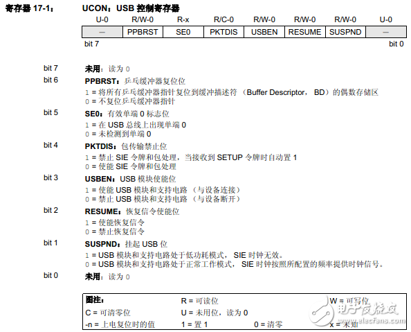
• USB Control Register (UCON): Used to control the operation of the module during transmission. This register contains configuration bits for control behavior. USBEN, you need to fully configure the module before you set this position. The PKTDIS bit, when received by the SETUP token, is set by the SIE to allow processing of SETUP. The microcontroller cannot set this bit to 1 and can only clear this bit to allow the SIE to continue transmitting and receiving. The RESUME bit allows the peripheral to wake up remotely by performing recovery signaling. For a valid remote wakeup, the firmware must set the RESUME bit and hold this state for 10 ms, then clear this bit. The SUSPND bit places the module and support circuitry (ie, the regulator) in a low power mode. The input clock of the SIE is also disabled. This bit must be set by software in response to an IDLEIF interrupt. This bit is reset by the firmware after the ACTVIF interrupt is generated. When this bit is active, the device is connected to the bus, but the transceiver output is idle. The voltage on the VUSB pin varies depending on the value of this bit. Setting this bit before the IDLEIF request will result in unpredictable bus behavior.
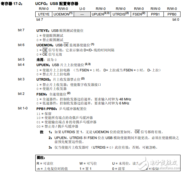
• USB Configuration Register (UCFG): The internal and/or external hardware associated with the module must be configured before communicating via USB. Most configurations are independent using the UCFG register. The USB regulator is also controlled through this configuration register. The control bits in the UFCG register can be used to control most of the system-level behavior of the USB module, including: • Bus speed (full speed and low speed) • On-chip pull-up resistor enable • On-chip transceiver enable • Ping pong buffer usage.
The internal transceiver, USB has a built-in USB 2.0 full-speed and low-speed compatible transceiver, connected to the SIE inside the USB. This feature is useful in low-cost single-chip applications. The UTRDIS bit controls the transceiver, which is enabled by default (UTRDIS=0). The FSEN bit controls the speed of the transceiver. Setting this bit enables the full speed mode of operation. The on-chip USB pull-up resistor is controlled by the UPUEN bit.
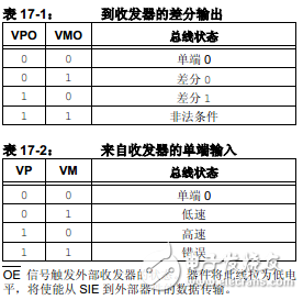
External transceiver, this module provides support for off-chip transceivers. An off-chip transceiver is used in applications where the transceiver is required to be remote from the SIE due to physical constraints. For example, an application that needs to be electrically isolated from USB can connect an external transceiver to the SIE of the microcontroller through some isolation component. The external transceiver can be enabled by setting the UTRDIS bit. There are 6 signal lines in the module to communicate with the external transceiver and control the external transceiver:
• VM: Single-ended D-line input (VM and VP signals report to the SIE that the serial bus cannot be captured with the RCV signal. The combined states of these signals and their descriptions are in Table 17-1 and Table 17-2. Listed.)
• VP: Single-ended D+ line input
• RCV: Differential Receiver Input (RCV signal is output from the external transceiver to the SIE, which converts the differential signal on the serial bus into a series of single pulse trains)
• VMO: differential line driver output (VPO and VMO signals are output by the SIE to an external transceiver)
• VPO: Differential Line Driver Output
• OE : Output Enable
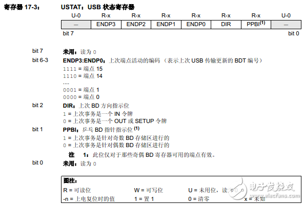
• USB Transfer Status Register (USTAT): The USB Status Register reports the status of the transaction in the SIE. When the SIE issues a USB transfer completion interrupt, the USTAT should be read to determine the status of the transfer. USTAT contains the transport endpoint number, direction of transmission, and ping pong buffer pointer value (if used). When the SIE finishes reading and writing data using the buffer, it updates the USTAT register. If another USB transfer is made before servicing the transaction completion interrupt, the SIE will save the state of the next transfer to the status FIFO.
• USB Device Address Register (UADDR): The USB Address Register contains a unique USB address that can be recognized by the peripheral when this address is valid. When a USB reset signal represented by URSTIF is received, or a reset message from the microcontroller is received, UADDR is reset to 00h. The microcontroller must write to the USB address during the USB boot phase (enumeration), which is supported by the Microchip USB firmware.
• Frame Number Register (UFRMH: UFRML): The Frame Number Register contains an 11-bit frame number. The low byte is stored in UFRML and the upper 3 bits are stored in UFRMH. The register pair is updated with the current frame number regardless of whether the SOF token is received. For microcontrollers, these registers are read-only. The frame number register is mainly used for synchronous transmission.
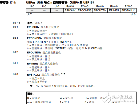
• Endpoint Enable Registers 0 through 15 (UEPn):
USB Endpoint Control: Each of the 16 available bidirectional endpoints has its own separate control register, UEPn (where n is the endpoint number). The function of the corresponding control bits in each register is the same. The EPHSHK bit controls the endpoint handshake. Setting this bit will enable the USB handshake. Usually, this bit is always set except for the sync endpoint. The EPCONDIS bit is used to enable or disable USB control operations (SETUP) through the endpoint. Clearing this bit enables the SETUP transaction; note that the corresponding EPINEN and EPOUTEN bits must be set to enable IN and OUT transactions. Because Endpoint 0 in the USB specification is the default control endpoint, this bit will always be cleared for Endpoint 0. The EPOUTEN bit is used to enable or disable the USBOUT transaction of the host. Setting this bit enables the OUT transaction. Similarly, the EPINEN bit will enable or disable the host's USB IN transaction. The EPSTALL bit is used to indicate the STALL state of the endpoint. If a particular endpoint issues a STALL, the SIE will set the EPSTALL bit of the pair to 1. This bit will remain set until cleared by firmware or by SIE.
USB RAM: USB data is transferred between the microcontroller core and the SIE through a memory space called USB RAM. The USB RAM is a special dual-port memory that is mapped to Bank 4 to Bank 7 (400h to 7FFh) in normal data storage space with a total capacity of 1KB. Bank 4 (400h to 4FFh) is dedicated to endpoint buffer control, while Bank 5 to Bank7 are available for USB data. Depending on the type of buffer used, all bytes can be used as USB buffer space except for the 8 bytes of Bank 4. Although the USB RAM can be used as the data memory of the microcontroller, the area accessed by the SIE cannot be accessed by the microcontroller. A signalling mechanism is employed here to determine access to a dedicated buffer at any given time.
Frame: The communication information on the bus is divided into multiple 1ms time slots, called frames. Each frame contains multiple transactions for multiple devices and endpoints.
Four transfer types are defined in the USB specification:
• Synchronization: This type of transfer ensures that large amounts of data are transferred in a timely manner (up to 1023 bytes), but the integrity of the data is not guaranteed. It is suitable for communication applications where loss of small amounts of data is not important, such as audio data.
• Bulk: This type of transfer allows for the integrity of data while transferring large amounts of data, but the transmission time limit is not guaranteed.
• Interrupt: This type of transfer ensures that small amounts of data are transmitted in a timely manner and that the integrity of the data is ensured.
• Control: This type provides device startup control. Full-speed devices support all transmission types, while low-speed devices can only use interrupt and control transmission.
Buffer descriptor and buffer descriptor table
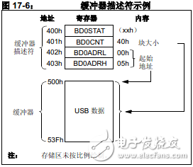
The registers in Bank 4 form a structure called the Buffer Descriptor Table (BDT), which is dedicated to controlling the endpoint buffer. This provides a flexible way for users to build and control endpoint buffers of various lengths and configurations. The BDT consists of a Buffer Descriptor (BD) that defines and controls the actual buffer in the USB RAM space. Each BD consists of four registers, where n represents one of 64 possible BDs (range 0 to 63):
• BDnSTAT: BD Status Register
• BDnCNT : BD byte count register
• BDnADRL : BD Low Address Register
• BDnADRH: BD high address register
BD always appears in the sequence as a four-byte data block BDnSTAT:BDnCNT:BDnADRL:BDnADRH), and the address of BDnSTAT is always an offset of 4n (in hexadecimal notation) relative to 400h, where n Is the buffer descriptor number. Depending on the buffering configuration used (Section 17.4.4 “Ping-Pong Bufferingâ€), there can be up to 32, 33 or 64 sets of buffer descriptors. The BDT must be at least 8 bytes long, as the USB specification states that each device must have the input and output endpoints 0 required for the initial boot. Depending on the endpoint and buffer configuration, the BDT can have 256 bytes.
Although it can be seen as a special function control register, the status and address registers of the buffer descriptor are not hardware mapped, which is different from the traditional microcontroller SFR in Bank 15. If the endpoint corresponding to a particular BD is not enabled, the endpoint's registers will not be used. It behaves as available RAM space, not an unimplemented address. These addresses can only be used as BD registers by enabling the endpoints by setting the UEPn '1' bit. As with any cell in the data memory area, the value of the BD register is undefined at device reset.
Figure 17-6 shows an example of a BD for a 40-byte buffer starting at 500h. If the corresponding endpoint has been enabled using the UEPn register, only certain BD register banks are valid. All BD registers in the USBRAM are available. The BD for each endpoint should be set before the endpoint is enabled.
BD Status and Configuration: The Buffer Descriptor not only defines the size of the endpoint buffer, but also determines its configuration and control. Most of the configuration is done via the BD status register BDnSTAT. Each BD has a numbered BDnSTAT register that corresponds to itself. Unlike other control registers, the setting of the bits in the BDnSTAT register is closely related to the specific application. There are two different configurations that determine whether a BD or a buffer is modified at a specific time to be a microcontroller or a USB module. Only one bit is shared by both configurations.
Buffer ownership: Because the CPU and USB modules share buffers and their BDs, a simple signaling mechanism is used to distinguish between CPUs and USBs that update BD and related buffers. UOWN (BDnSTAT "7") can be used as a signal to distinguish. UOWN is the only bit shared between the two configurations of BDnSTAT.
When UOWN is cleared, BD is "owned" by the microcontroller core. When the UOWN bit is set, the BD and buffer modules are "owned" by the USB peripherals, at which point the kernel cannot modify the BD or the corresponding data buffer. Note that the microcontroller core can still read BDnSTAT when the SIE has a buffer, and vice versa.
Buffer descriptors have different meanings depending on the update source of the registers. The user can configure the basic operation of the peripherals via BDnSTAT before assigning ownership to the USB peripherals. At this time, the byte count and buffer address registers can also be set.
When UOWN is set to 1, the user can no longer rely on the value of writing BD. At this time, the SIE updates the BD as needed, and rewrites the original BD value. The SIE will use the PID token to update the BDnSTAT register and will also update the transfer count value BDnCNT. The BDT's BDnSTAT byte is always the last updated byte before the endpoint is ready to be set. When the transaction is completed, the SIE will clear the UOWN bit. The only exception is when KEN and / or BSTALL are enabled. When the UOWN bit is set, there is no mechanism on the hardware to prevent the microcontroller from accessing the memory area. Therefore, if the microcontroller attempts to change the memory area while the SIE has USB RAM, unpredictable consequences may occur. Similarly, reading the memory area may cause data errors before the USB peripheral returns the USB RAM ownership to the microcontroller.
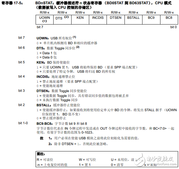
BDnSTAT register (CPU mode): When UOWN = 0, the microcontroller core has BD. At this point, the other seven bits of this register are control bits. The hold enable bit KEN (BDnSTAT "5") determines the ownership of the BD ownership. If this bit is set, once the UOWN bit is set, the BD will remain owned by the SIE regardless of the endpoint activity. This will prevent the USTAT FIFO from being updated while preventing the endpoint's transaction completion interrupt flag from being set. This feature is only enabled when the parallel port is selected instead of USB RAM as the data I/O channel.
The address increment disable bit INCDIS (BDnSTAT "4") controls the automatic address increment function of the SIE. Setting INCDIS to 1 will disable the SIE from automatically incrementing the buffer address when transmitting or receiving each byte. This feature is enabled only when the SPP port is used, in which case each data byte is sent to or from the same location.
The data Toggle sync enable bit DTSEN (BDnSTAT "3") controls the parity of the data transfer. Setting DTSEN to 1 enables the SIE data Toggle synchronization and verifies the parity bit of the packet against the value of DTS (BDnSTAT "6"). If the packet does not arrive synchronously, the data will be ignored, will not be written to the USB RAM, and the USB Transaction Complete Interrupt Flag will not be set. The SIE will send an ACK token back to the host to respond to the receipt. Table 17-3 summarizes the impact of the DTSEN bit on the SIE.

The buffer stop bit, BSTALL (BDnSTAT "2"), provides support for control transfers, usually only once at endpoint 0. It also supports the SET_FEATURE/CLEAR_FEATURE command specified in Chapter 9 of the USB Specification, which is a unique continuous STALL for any endpoint outside the default control endpoint.
The BSTALL bit enables the buffer to stop. If the received token is to use the BD in the unit, setting BSTALL will cause the SIE to return the STALL token to the host. The EPSTALL bit in the corresponding UEPn Control Register is set and a STALL interrupt is generated when STALL is sent to the host. The UOWN bit remains set and the BD does not change unless a SETUP token is received. In this case, the STALL condition is cleared and the ownership of the BD is returned to the microcontroller core.
BD9: The BD8 bit (BDnSTAT "1:0") stores the upper 2 bits of the SIE byte count, and the lower 8 bits are stored in the corresponding BDnCNT register.
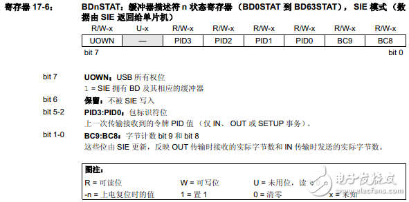
BDnSTAT register (SIE mode): Most of the bits in BDnSTAT have different definitions when the BD and its buffers are owned by the SIE. The configuration is shown in Register 17-6. Once UOWN is set to 1, any data or control settings previously written by the user will be overwritten by the data from the SIE. The SIE updates the BDnSTAT register using the Packet IdenTIfier (PID), which is stored in BDnSTAT "5:3". The transfer count in the corresponding BDnCNT register is updated, and the upper two bits of the count value obtained by overflowing the value of the eight-bit register are stored in BDnSTAT "1:0".
BD Byte Count: The byte count represents the total number of bytes that will be sent during an IN transmission. After the IN transfer, the SIE will return the number of bytes sent to the host. During the OUT transfer, the byte count represents the maximum number of bytes that can be received and stored in the USB RAM. After the OUT transfer, the SIE will return the actual number of bytes received. If the number of bytes received exceeds the set byte count, the packet will be rejected and a NAK handshake will be generated. When this happens, the byte count is not updated.
The 10-bit byte count is saved to two registers, respectively. The lower 8 bits are in the BDnCNT register. The upper 2 bits are in BDnSTAT "1:0". Therefore the valid byte count range is 0 to 1023.
BD Address Verification: The BD address register pair contains the starting RAM address of the corresponding endpoint buffer. In order for the endpoint start unit to be valid, it must be in the USB RAM (address 400h to 7FFh). There is no corresponding mechanism in the hardware to verify the BD address. If the BD address does not point to a location in the USB RAM, or to an address in another endpoint buffer, the data will most likely be lost or overwritten. Similarly, the overlap of the receive buffer (OUT endpoint) and the BD unit being used will also lead to unpredictable results. When developing a USB application, the user needs to consider verifying the address in the software.
Ping Pong Buffer: When an endpoint has two sets of BD entries (one for even data transfers and one for odd data transfers), it is defined as having a ping pong buffer. This allows the SIE to process another set of BDs while the CPU is processing a set of BDs. This type of ping-pong buffer BD can achieve the maximum data throughput between the microcontroller and USB.
The USB module supports three modes of operation:
• Does not support ping pong buffering
• Only ping-pong buffers that support OUT endpoint 0
• Support for ping pong buffering for all endpoints
The ping pong buffer is set using the PPB1:PPB0 bits in the UCFG register. The USB module tracks the ping-pong pointer for each endpoint. When this module is enabled, all pointers are reset to point to even BDs. After the transaction is completed (UOWN is cleared by SIE), the pointer is switched to odd BD. After the next transaction is completed, the pointer is switched back to even parity. The parity state of the last transaction of the BD is stored in the PPBI bit of the USTAT register. The user can reset all ping-pong pointers to an even state using the PPBRST bit. Figure 17-7 shows three different modes of operation and how BD fills the USB RAM. According to the buffer configuration, the BD has a fixed correspondence with a specific endpoint. Table 17-4 shows the details of the mapping between BD and endpoints. This relationship also means that if the endpoint is not continuously enabled, a blank area will appear in the BDT. A BD of a theoretically prohibited endpoint can be used as a buffer space. In fact, users should avoid using these spaces in the BDT unless they have taken steps to verify the BD address.
USB interrupt: The USB module can generate multiple interrupt conditions. To identify all interrupt sources, like a microcontroller, this module has its own interrupt logic structure.
USB Power Mode: The most common power modes are Bus Power Only, Self-Power Only, and Self Power-based Dual Power.
Parallel Communication Port: The Parallel Communication Port (SPP) is an alternate channel for data transfer in addition to the USB RAM. The endpoint can be configured to use SPP to send data directly to external hardware or directly receive data from external hardware.
This method can use the MCU as a data manager to directly transfer large blocks of data through the SPP without the need for a single chip to process. The application example will include a data acquisition system where the external FIFO data passes through the USB and host
Communicate. In this case, the microcontroller controls the endpoint, and the transfer of the original data is done by the peripheral. The SPP is enabled as a port for the USB endpoint through the associated endpoint buffer descriptor. The endpoint must be enabled by:
1. Set BDnADRL:BDnADRH to point to FFFFh.
2. Set the KEN bit (BDnSTAT "5") to 1 to allow the SIE to maintain control of the buffer.
3. Set the INCDIS bit (BDnSTAT "4") to 1 to disable address auto-increment.
Oscillator: The USB module has specific clock requirements. In full speed mode, the clock source must be 48 MHz. Even so, the microcontroller core and other peripherals are not required to run at this clock speed or use the same clock source.
USB firmware and drivers: Microchip provides specific resources for the application, such as USB firmware and drivers.
KNLE1-63 Residual Current Circuit Breaker With Over Load Protection
KNLE1-63 TWO FUNCTION : MCB AND RCCB FUNCTIONS
leakage breaker is suitable for the leakage protection of the line of AC 50/60Hz, rated voltage single phase 240V, rated current up to 63A. When there is human electricity shock or if the leakage current of the line exceeds the prescribed value, it will automatically cut off the power within 0.1s to protect human safety and prevent the accident due to the current leakage.
leakage breaker can protect against overload and short-circuit. It can be used to protect the line from being overloaded and short-circuited as wellas infrequent changeover of the line in normal situation. It complies with standard of IEC/EN61009-1 and GB16917.1.
KNLE1-63 Residual Current Circuit Breaker,Residual Current Circuit Breaker with Over Load Protection 1p,Residual Current Circuit Breaker with Over Load Protection 2p
Wenzhou Korlen Electric Appliances Co., Ltd. , https://www.zjaccontactor.com