If you have a background in software engineering and want to find a job as a digital design engineer, the first thing you need to do is to learn the clock concept as early as possible. For many junior hardware design engineers who are transferred from software engineers, the clock concept is annoying. Without a clock, they can convert HDL (Hardware Description Language) into a programming language such as $display, if, and for loops, just like any other programming language. However, the clocks that these junior designers ignore are often the most fundamental part of digital design.
There are times when there are more problems than when examining the products that the primary HDL design engineer designed for the first time. Now, I have spoken to several people who have posted questions on the forums I participated in. When I got to know more and found out what they were doing, I felt embarrassed for them.
Taking a student as an example, he does not understand why no one on the network values ​​the HDL implementation of his Advanced Encryption Standard (AES). Here, in order not to let him be embarrassed because of his name or project, he will be called a student for the time being. (No, I am not a professor.) This "student" created a Verilog design that performs more than one round of AES encryption, but each round is combinatorial logic with no clock between them. I don't remember if he was doing AES-128, AES-192 or AES-256, but AES needed 10 to 14 rounds of calculations. I remember that his encryption engine works flawlessly in the emulator, but he only uses one clock to encrypt or decrypt his data. He is proud of his work, but he doesn't understand why anyone who has seen this project tells him that he thinks like a software engineer, not a hardware designer.
In fact, I now have the opportunity to explain the doubts to HDL novice software engineers like this “studentâ€. Many of them treat the HDL language just like another software programming language. Before programming, they went looking for the basics of any software programming language: how to declare variables, how to create an if or case statement, how to write loops, and more. Then, writing code is like writing a computer program—everything is sequential (Figure 1), and completely ignores the basic fact in digital design that all operations are parallel.
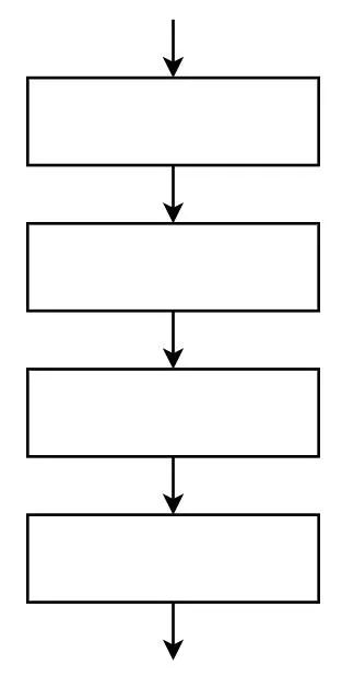
Figure 1: Software execution is sequential
Sometimes these programmers use simulators such as Verilator, iverilog or EDA platforms. They then use a bunch of $display commands in the logic code to treat them as sequential "printf" and use these commands to run the code instead of using the clock. Their design is simply "executed" in combination logic in the simulator.
These students described their design to me and explained that their design "can be executed without a clock."
God, what are these thoughts?
In fact, any digital logic design will not work without a clock. There are always some physical processes that create input. These inputs must be valid at some start time - this time forms the first clock scale in their design. Similarly, it is output after receiving these inputs for a period of time. For a given set of inputs, the effective time of all outputs forms the next "clock" in the "no clock" design. Perhaps the first clock scale is when they adjust the last switch on the board, and the last clock scale is when they read the result. It doesn't matter how the clock is formed: there is a clock.
The result of this is that those who claim that their design "has no clock" explain that he is using the simulator in an impractical way, or that there is an external clock in the design for setting the input and reading the output - and this Another way is to show that there is indeed a clock in the design.
If you find yourself trying to understand digital logic in this way, you must have a clock to execute, or someone you know tries to understand, so this article is for you.
Next, let's spend a minute or two discussing the clock and why it's important to build and design your digital logic around the clock.
Hardware design is parallel
The first and most difficult part of hardware design learning is that the hardware design is a parallel design. All code instructions are not executed sequentially, as if one instruction was connected to the next (as shown in Figure 1), just like a computer program. Instead, all instructions are executed at the same time, as shown in Figure 2.

Figure 2: Hardware logic running in parallel
It is this that makes a lot of things different.
The first thing that needs to change is the developer. You need to learn to think in parallel.
A hardware loop might be a good example if you want to illustrate the difference between the two.
In software design, a loop consists of a series of instructions, as shown in Figure 3. These instructions construct a set of initialization conditions, and the actual logic is executed inside the loop. Construct and define a loop logic by using a loop variable, and this variable is usually incremented in each loop. The computer CPU repeatedly executes the instructions and logic in the loop until the loop variable reaches the termination condition. The more cycles you run, the longer it will run in the program.
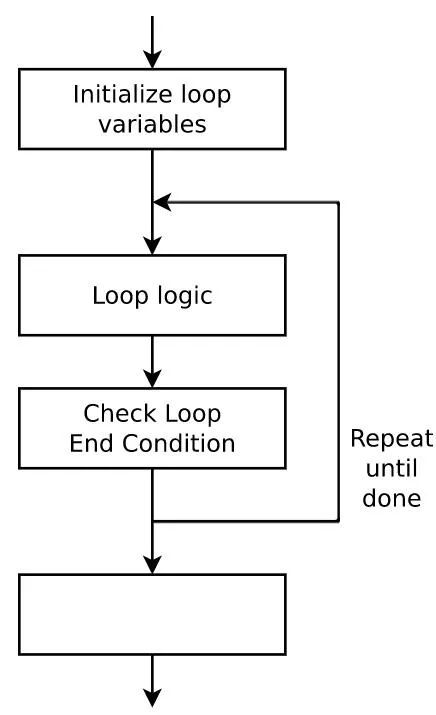
Figure 3: Software Loop
The hardware-based hardware description language loop is completely different from the software loop. Quite the contrary, the HDL synthesis tool uses loops to make copies of all logic run in parallel at the same time. The code used to construct the loop logic, such as defining the index, index growth, checking whether the index reaches the termination condition, etc., does not need to be synthesized and is usually removed. Furthermore, since the synthesis tool is building physical lines and logic blocks, the number of execution cycles cannot be changed after the synthesis time. After that, the number of hardware is fixed and cannot be changed.
The result is that the hardware loop structure (shown in Figure 4 below) is quite different from the software loop structure (shown in Figure 3 above).

Figure 4: HDL loop
This has several consequences. For example, hardware loop iterations differ from software loop iterations in that it does not have to rely on the output of previous loop iterations. The result of this is that running a logical loop containing a set of data is hard to get a response on the next clock.
But... now let's go back to the clock concept.
The clock is at the heart of any FPGA design. Everything revolves around it. In fact, I think all logic design development should start with the clock. The clock shouldn't be added after the design is complete, but when you start thinking about how to design the architecture.
Why is the clock important?
In the first step, you need to understand that everything in digital logic design takes time to execute on hardware. Not only that, but the total amount of time required for different operations is also different. It takes time to move from one part of the chip to another.
Perhaps this can be explained more intuitively by means of a chart. We put the input at the top of the algorithm, the logic in the middle, and the output at the bottom. Time is the axis, running from top to bottom, from one clock to the next. This visual effect looks like the one shown in Figure 5 below:
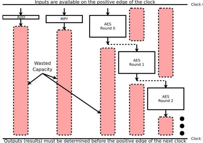
Figure 5: Logic time for three operations
Figure 5 shows several different operations: addition, multiplication, and multiple rounds of AES algorithms—although for the purposes of discussion, it can be any number of other algorithms. I used the size of the box vertically to indicate how much time might be required for each operation. In addition, the blocks that depend on other operations are stacked. So if you want to do a lot of rounds of AES in a clock, you have to understand that the second round of algorithms won't start until the first round of the algorithm ends. Therefore, adapting to this logic will increase the time interval between clocks and slow down the overall clock frequency.
Let us now pay attention to this pink box.
This pink box indicates the wasted ability to run in the hardware circuit, which is the time you could have used to do more things, but because you need to wait for the clock, or wait for the input to be processed, you can't do anything. For example, in the above conceptual diagram, the time taken to complete the multiplication operation does not require a long round of AES algorithm, and the addition is also. However, when the AES algorithm is executing, you cannot perform any actions on the results of these two operations, because these operations need to wait for the next clock to get their next input. This is what the pink box in Figure 5 expresses: the idle circuit. In addition, since each round of AES algorithm delays the arrival of the next clock, there are a large number of idle circuits in Figure 5. Therefore, the design will not run as fast as the hardware allows.
If we only use the AES algorithm, then each clock just completes a round of AES calculations. As a result, you can reduce the waste of running capacity and make the entire design run faster.
Figure 6 shows this design idea.
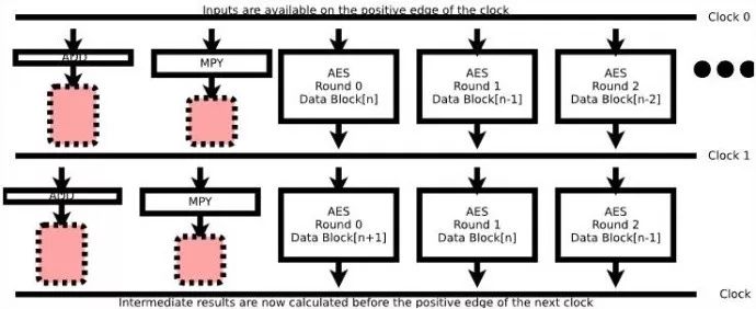
Figure 6: Decomposition operation speeds up the clock frequency
Since we break down the operation into smaller operations, each can be done in a clock unit, so we've improved our ability to run. Even we can pass a pipe encryption algorithm instead of just encrypting one block at a time. The result of this logic design will not be faster than shown in Figure 5 above, but if you can keep the pipeline full, you can increase the AES encryption throughput to between 10-14x.
Therefore, this design is more like.
Can there be other better solutions? of course! If you are familiar with AES, you know that there are separate steps in each round of AES calculations. These steps can be decomposed again so that the overall clock speed of each round of logic algorithms can be increased again. This can increase the number of additions and multiplications you can perform, as well as the micropipes of the crypto engine so that you can run more data on a per clock basis.
The design is good.
However, there are other things in Figure 6 above.
First, the arrow indicates the routing delay. (This number is not drawn to scale. It is just an example of this discussion example.) Each piece of logic requires a piece of logic to pass the result to it. This means that even if a certain logic block does not require time to execute - for example, just rearranging lines or the like, it takes time to move the logic blocks from the end of one chip to another. So, even if you simplify the operation, there is still a delay in the delivery of each round of data.
Second, you may notice that no arrow starts at the clock scale, that is, no logic block runs until the next clock begins. This is to demonstrate the concept of startup time and maintenance time. The flip-flop circuit, a circuit structure that captures data and synchronizes to the clock, takes a certain amount of time before the next clock arrives, at which point the data is already fixed and deterministic. Also, although the clock is usually considered instantaneous, it is never. It reaches different parts of the chip at different times. This again requires some buffering between operations.
Through the above discussion, what conclusions can we draw?
The logic implementation takes time.
The more logic, the more time it takes.
The sum of the time taken to complete the logic between the two clock scales (including routine delays, start and hold times, clock uncertainty, etc.) limits the clock speed. The more logical processing between clocks, the slower the clock rate.
The clock speed required to complete the slowest operation limits the speed of the fastest operation. As in the addition operation in the above example. It can perform faster than multiplication and any single round of AES algorithms, but its speed is slowed down by the rest of the logic in the design.
The hardware definition also limits the clock speed. Even if the operation does not contain any logic, it takes time.
Therefore, balanced design attempts to place a large amount of the same logic between clocks throughout the design.
How much logic should I put between the clocks?
Now that you know that you have to deal with the clock, how do you modify and conceive your design based on the above information? The answer is to limit the amount of logic between clocks. But the question is, what is the quantity? How do you get this amount?
One way to figure out how much logic you can place between clocks is to set the clock speed to any speed and then build your design in the tool suite that comes with the hardware you need. Whenever your design fails to meet its timing needs, you need to go back and split the components in your design or slow down the clock. By using the design tools, you will eventually be able to find the longest path.
If you do this, you will learn some exploration methods yourself, and then by using these methods, you can find the exact amount of logic that can be placed between the clocks of the running hardware.
For example, I tend to design 100MHz clock rates in Xilinx 7 series parts. These designs typically run on Spartan-6 at a rate of approximately 80MHz, or on a 50MHz iCE40 - although these are not hard relationships. Putting a program that is normally executed on one chip on the other may be overloaded, or the clock check may fail.
Here are some rough exploratory experiences I have gained while using the clock. Due to their personal experience, these methods are not suitable for all designs:
1. Usually, when I design a 32-bit addition, I use a multiplexer with 4-8 entries in one clock.
If you want to use a faster clock, such as a frequency of 200 MHz, you may need to strip the addition from the multiplexer.
The longest path to the ZipCPU is actually the input from the ALU's output to the ALU.
It sounds simple. It even conforms to the previous rules of thumb.
But the problem with ZipCPU is how to route the output back to the input at a faster speed.
Let's trace this path: Following the ALU, the logical path first determines whether the ALU is through a 4-way multiplexer, and the memory or crossover output needs to be written back. The writeback result is then fed into the bypass circuit to determine if it needs to be immediately passed into the ALU as one of its two inputs. The multiplexer is only generated at the end of the multiplexer and the bypass path performs the ALU operation. Therefore, all of these logical steps put pressure on the ALU. However, due to the design of the ZipCPU, any clock on this route may slow down the ZipCPU speed. This means that it is possible that this longest line is still the longest line in the ZipCPU.
I was interested in running ZipCPU at a higher speed, which is the first logical path I tried to decompose and optimize.
A 2.16 x 16-bit multiplier requires a clock.
Sometimes, on some hardware, I can run 32x32 bit multiplication on a single clock. On other hardware, I need to break down this operation. So if I need a signed 32x32 bit multiplication, I use the pipeline routine I built specifically for this. This routine contains several of these multiplication methods, allowing me to choose from the options that are appropriate for the hardware I am currently working on.
Your hardware may also support 18×18-bit multiplication. Some FPGAs also support multiplication and accumulation within an optimized hardware clock. As long as you are familiar enough with the hardware you are using, you know what you can do with it.
3. A clock is required to access any RAM block.
If possible, try to avoid adjusting the index during this clock cycle. Again, avoid doing anything about the output during this clock.
Although I think this is a good rule, I have violated two of them on the 100MHz Xilinx 7 series device without causing (serious) effects. (There is a problem on the iCE40 device.)
For example, the ZipCPU reads data from a register, adds an immediate value to the result, and then chooses from the results whether the immediate value should be added to the register, PC, or condition code register—all within one clock.
Another example is that the Wishbone Scope has long determined the address read from the buffer based on whether the current clock is being read from memory. To interrupt it from this dependency, you need to add another delay clock, so the current version will no longer destroy this (self-imposed) rule.
These rules are just a method of experience that I have accumulated over time to determine the amount of logic that can be accommodated in a single clock. These rules of thumb are related to device and clock speed, so they may not be suitable for your design development. I suggest you accumulate your own exploration experience so that you know what to do between clock cycles.
Next step
Perhaps the final recommendation I can offer to any new FPGA developer is to practice on HDL when learning HDL, not just on the simulator. A tool associated with the actual hardware components that excels at checking code and calculating the time required. In addition, the idea of ​​building a design with a high-speed clock is good, but this is not the end result of hardware design.
Remember, the hardware design is parallel. Everything starts with the clock.
24HR Electronic timer socket with photocell.
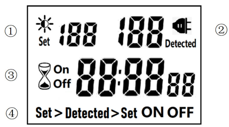
â‘ Light intensity setting
â‘¡ Light intensity detection
â‘¢ Countdown Timer ON & OFF
â‘£ 4 MODES:
Set > Detected: When the light intensity detection value is less than the set value, switch ON or OFF.
Detected > Set: When the light intensity detection value is greater than the set value, switch ON or OFF
ON : Always ON
OFF : Always OFF
NOTED:
1. The light intensity displayed by this machine is not the standard light intensity value (Lux), only the relative light intensity value.
2. The light intensity value is affected by the placement position and direction. Please determine the position first and then set it according to the actual light intensity detected. If you change the position or change the orientation, you need to reset the light intensity setting value suitable for the new position.
3. This product has built-in rechargeable battery. If it is not connected to AC for a long time, you need to connect the power supply to charge until the LCD can display normally.
MANUAL OPERATION
1. Press [UP" or [DOWN" to set the LUX value.
2. Press the [SET" key to start setting, and the P1 settable items will be flashed.
3. Press [UP" or [DOWN" to adjust the value.
4. Press [SET" key again to exit setting or enter next setting for countdown timer.
5. Repeat the [SET" key to start setting, and the P2 & P3 settable items will be flashed.

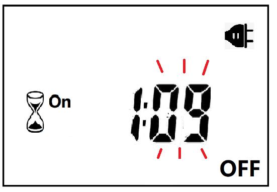

6. Press the [FUN" key to switch the working state in the following:
Set > Detected -> Detected > Set -> ON -> OFF
Set > Detected: Automatically switches when the detected ambient light intensity is darker than the set value
Detected >Set: Automatically switch when the detected ambient light intensity is brighter than the set value
When the brightness meets the setting conditions, the countdown starts as below:
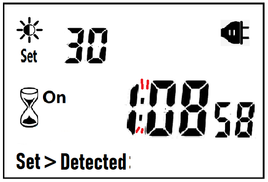
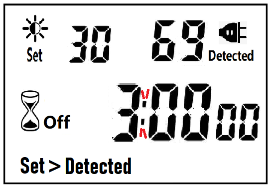
Note:when the countdown is ON, the detected value is not displayed.
When the brightness does not meet the setting conditions, the countdown stops and waits:
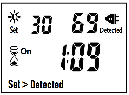
After the countdown ON is reduced to 0, the countdown OFF starts immediately and the power is OFF.
After the countdown OFF is reduced to 0:
A. If the light intensity meets the set conditions, a new round of countdown will be started;
B. If the light intensity does not meet the set conditions, keep the power off and wait for the light to meet the conditions before turning on automatically.
NOTE:
1. If the power is cut off while the countdown is running, the countdown will be terminated immediately and the relay output will be off. After the power is turned on again, a new round of brightness detection will start.
2. Modifying the brightness value in the countdown operation will not affect the current countdown operation. After the off time of the current countdown, the new brightness setting value will take effect.
3. In the countdown on operation, change the setting value of the countdown on, this countdown will still be timed according to the original setting value; the new setting value will take effect when the next countdown on starts.
4. In the countdown off operation, change the setting value of countdown off, this countdown will still be timed according to the original setting value; the new setting value will take effect when the next countdown off is started.
NOTE: the brightness setting value, countdown ON or countdown OFF, any one of which is equal to 0, cannot be switched ON or OFF automatically.
Manual Control
When ON or OFF is displayed, it means that the power supply remains ON or OFF, as shown in the figure below:

Power Detection and Standby Mode
With AC power supply, the icon ![]() lights up and works normally.
lights up and works normally.
When there is no AC power supply, the icon ![]() goes out, the brightness is not detected at this time, and the system enters the standby mode.
goes out, the brightness is not detected at this time, and the system enters the standby mode.
Photocell Timer, Photocell Timer Socket, Photocell Sensor, Photocell Sensor Socket, Sensor Plug, Sensor Switch Socket, Digital Photocell Timer, Digital Sensor Timer
NINGBO COWELL ELECTRONICS & TECHNOLOGY CO., LTD , https://www.cowellsockets.com