At the 2017 Q4 Law Conference held recently, TSMC revealed that its ultra-violet lithography (EUV lithography) capacity has made great progress, and its power supply has been improved. Up to 160W, 7nm and 5nm manufacturing, and 250W EUV is already in place.
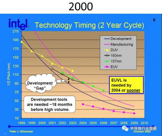
ASML, the sole supplier of EUV lithography machines, also said at the 2017 Semicon West Semiconductor Equipment Show that the 250-watt EUV light source is also well-equipped. The company's 2017 financial report also emphasized that its EUV lithography machine meets the performance specifications of 125WPH (125 wafers per hour). That means that the EUV lithography machine originally planned for launch in 2004 was finally ready after 13 years of delay.
EUV lithography machine is known as the savior, the key problem has been solved
In the past few decades, the semiconductor industry has achieved rapid development under the guidance of Moore's Law. In order to meet Moore's Law, “The number of transistors integrated in the same area of ​​chips is doubling every 18 monthsâ€, the fab has been promoting the process. Update. However, with the evolution of nodes, the industry generally believes that traditional lithography will suffer obstacles at 65nm or 45nm, so they are looking for new solutions, EUV is their main choice.

The term "EUV" refers to light having a wavelength of 13.5 nm. Compared to the 193nm light source used in mainstream lithography machines, the new EUV light source can engrave a smaller channel for the silicon wafer, thereby enabling more transistors to be integrated on the chip, thereby improving chip performance and continuing Moore's Law. However, in the process of advancing the EUV lithography machine, various kinds of problems were encountered, and the commercial time of the EUV lithography machine was delayed. The industry's R&D investment in the EUV was conservatively estimated to exceed 20 billion US dollars. The source power of the illuminating light is the most important cause of the delay in commercial use of the EUV lithography machine.
During the operation of the EUV lithography machine, the power source is required to convert the plasma into light of 13.5 nm wavelength, and then pass through several reflections of the mirror and then drop it onto the wafer. But the previous power supply did not provide enough power for the EUV to meet economic viability. This is the first thing to understand the requirements for EUV lithography machines:
To put it simply, the goal of introducing an EUV lithography machine is to simplify the double-layer pattering of the conventional lithography into a layer of EUV, thereby reducing the number of layers of the reticle and reducing the production complexity. In order to achieve the production efficiency of the existing conventional lithography machine from 250 to 270 WPH, then to the EUV lithography machine, at least 125 WPH efficiency is required to achieve COO (cost of ownership) and OEE (overall equipment efficiency). A 250 watt requirement is imposed on the light source. But knowing that in 2012, ASML, the only supplier of EUV lithography machines, only realized a 25 watt light source.

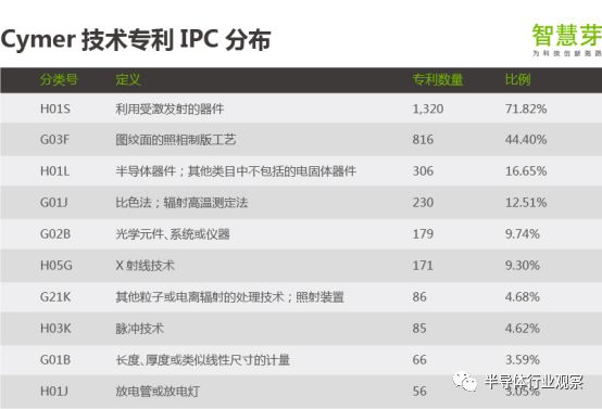
In order to accelerate the development of light sources, they spent $2.5 billion in 2012 to acquire Cymer, the world's leading provider of excimer laser sources. From the wisdom of the world's leading patent enquiry platform, Cymer is a company specializing in laser, X-ray and deep ultraviolet light sources. The acquisition of Cymer allowed ASML to directly acquire the lithography source technology that is crucial in its development from the source. This has accelerated the development of EUV lithography machines.

According to reports, Cymer uses a method called “laser plasmaâ€, which uses a magnifier derived from metal cutting technology to generate a powerful carbon dioxide laser through a cavity and illuminate a beam in a vacuum chamber. 50,000 drops of ultrapure tin droplets were emitted per second. When a laser pulse is irradiated onto the tin droplet, the droplet is heated into a plasma and generates EUV rays. Next, a mirror collector reflects the light generated by the process into the lithography machine.
Based on this method, ASML and Cymer continue to improve and reach 200 watts of power in 2016. By the second half of 2017, 250 watts of light source and 125 WPH efficiency have finally been realized, which means that EUV lithography machine Commercial is just around the corner.
The battle for Samsung, TSMC, Intel and Gexin started
With the development of HPC and smart phones, the requirements for chip performance are getting higher and higher, and the demand for advanced technology by design manufacturers is also rising. In TSMC's Q4 law, TSMC said that it has 50 7nm customers, which is the most Good proof. Faced with this market, as stated at the beginning of the article, wafer foundries need to look to EUV lithography machines for help. The Samsung fab, which was just out of the Samsung Group in May 2017, is the most radical one.
Samsung said that they are the first in the industry to announce the use of EUV lithography machines for 7nm chip production. According to Samsung, they will provide related services in the second half of 2018. As for TSMC, according to sources in the supply chain, TSMC will start production at 7nm at the end of the second quarter, but the first generation of 7nm will use traditional lithography. . TSMC said that EUV will be introduced until 7nm plus in 2019; Gexin also plans to introduce 7nm technology in 2018, but like TSMC, it still uses traditional lithography, and they plan to introduce EUV by 2019. As for the IDM giant Intel, they are secretive about the progress of their advanced technology and EUV, but according to public information, they have purchased more EUV lithography machines than any other company.
EUV lithography machine is undoubtedly the trend of the future.
Gary Patton, CTO of Gexin, said that if EUV lithography is not used at 5nm, the lithography step will be more than 100 steps, which will make people crazy. Therefore, the EUV lithography machine is undoubtedly the most important production tool for the future 5nm and 3nm chips, and the battle for EUV lithography machines in the future will become extremely fierce. Because this is the key to determining the future competition of these manufacturers in the advanced process market.
According to media reports, TSMC ordered five EUV lithography machines at the beginning of 2017. Korean media BusinessKorea also said in October that Samsung intends to purchase 10 EUV lithography machines. There are no reports on the specific purchases of grid cores and Intel lithography machines. But from the perspective of S and T, they are making big purchases. However, ASML's capacity on EUV lithography machines is not large, which may intensify competition.
According to ASML's annual report, in 2016, they shipped a total of four EUV lithography machines, and in 2017 they delivered 10 EUV systems. From the media reports, we know that in 2018, ASML's EUV lithography machine can reach 24 units, but these orders have been snapped up. But by 2019, ASML will increase its production capacity to 40 units, which will greatly ease the supply pressure of EUV lithography machines.
Bigger challenges are thrown behind
After fundamentally overcoming the 250W source problem, ASML has a basic account for fab customers, but there are still some issues that need to be addressed for EUV lithography systems.
The first is the mask problem;
According to reports, the reticle used in EUV is completely different from the 193 nm immersion lithography mask, which consists of nano-layers using dozens of different materials. According to data surveys, mask manufacturers have produced 1,041 EUV masks in the past 12 months, and the mask yield is currently only 64.3%. However, the number of mainstream masks exposed during the same period reached 461,792, and the average yield was as high as 94.8%. Therefore, how to improve the mask yield and cost is the primary issue they consider.
Secondly, the EUV film problem can not be ignored;
Although EUV equipment is now in an ultra-clean environment, dust is inevitably generated during the manufacturing process. If there is a bit of returning to the city, it will cause a lot of damage. Nowadays, the film of the mainstream mask is transparent and can withstand the test, but the current EUV film is opaque, so the ultra-thin film is needed to manufacture the transparent EUV film, which can resist the shock and correlation of the EUV lithography machine. The effect of interference on the reticle.
Another important issue is that there is currently no good way to detect defects in the reticle;
Ideally, you can use EUV light to scan for points that need to be patched. But this technology, called actinic patterned-mask inspection, is still under study, so all chip makers can only use expediency in reticle inspection: some manufacturers use 193nm lithography tools. But when it comes to 7nm, the method of using 193nm is no different from the fish. Because the methods are the same, you will always miss something. Chip makers also use a technique called "print check" to inspect wafers, but this method is costly and time-consuming and unacceptable.
For ASML, there is still a need to solve a light source problem in the future.
The current 250W light source application is no problem at 7nm or even 5nm, but by 3nm, the power demand for the light source will reach 500W. When it reaches 1nm, the power requirement of the light source even reaches 1KW, which is not an easy one. problem.
Let me expect some smart engineers to help us solve these problems.
12 Coaxial Speaker,Coaxial Speaker 12 Inch,12 Inch Coaxial Speaker,Pro Audio Coaxial Speakers
Guangzhou Yuehang Audio Technology Co., Ltd , https://www.yhspeakers.com