Next month, Moore's Law, the principle that the global semiconductor industry has followed since the 1960s, will be blown to the death horn, which also means the end of the information technology revolution.
Moore's Law is a speculative rule of thumb:
The number of transistors on a microprocessor chip will double every two years or so, and this usually means that the performance of the chip will also be doubled.
The law of exponential growth described in this law was not only confirmed in the history of home computer development in the 1970s and 1990s, but also in the development of the Internet, smart phones, automobiles, refrigerators, thermostats and other industries. .
However, all this is not inevitable: Take the chip industry as an example. In every stage of development, software developers will provide consumers with applications that squeeze the performance of existing chips, boost consumer demand for performance, and promote Chip makers are stepping up their efforts to develop next-generation chip devices with even better performance to meet demand.
Not only that, since the 1990s, the semiconductor industry has released a research roadmap every two years to ensure that hundreds of manufacturers and suppliers in the industry are in tune with Moore's Law. To a large extent, the reason why the entire home-computer industry is able to follow the law in an orderly manner is largely due to the unified planning of such a roadmap.
Although chip makers hope to continue on the track of Moore’s Law, the physical bottleneck of silicon processors is a problem that will sooner or later.
As more and more silicon circuits are integrated into such a small area, the development law that has doubled in every two years has started to stagnate. The current high-end microprocessors have reached the 14nm process level, which is less than the size of most viruses. It is expected that silicon processors will reach their physical limits in the next decade.
“Even under the premise that the entire industry continues to make breakthroughs in R&D, we will still reach the 2–3nm chip process limit in the early 1920s.â€
- Paolo Gargini, chairman of the "Road Map" organization
If we further reduce the size of the process, the behavior of the electrons will be affected by the quantum uncertainty, making the transistor unreliable. Although research work has been ongoing, there is currently no successor to silicon technology.
The semiconductor industry will announce plans for R&D routes next month, but it is worth noting that this is the first time the organization has no longer established a roadmap based on Moore's Law. Instead, this will follow the so-called "Moremore Moorestrate strategy": Instead of driving application development with chip technology, application needs will be the driving force.
Small to smart phones, large to supercomputers, and cloud data centers, the future will be based on their needs to determine the development of the chip. These chips will become a new generation of sensors, power management circuits, and other required silicon devices, and future computing will become increasingly mobile.
But in this way, Moore's Law, which has dominated the electronics industry for more than 50 years, will also be broken. The United States Semiconductor Industry Association (SIA) has represented all the major U.S. companies in the industry that after the next month’s report is released, it will no longer participate in the formulation of the roadmap. In the future, the association will shift to its own research and development agenda.
However, the end of Moore's Law does not mean the end of technological development.
“Everyone is wondering what the roadmap really means. In fact, we can compare the aircraft industry: Although the Boeing 787 did not fly faster than the Boeing 707 in the 1950s, they are definitely two different eras. The aircraft - Boeing 787's technological innovation lies in all-electronic control and carbon fiber body.This will also be the future of the PC industry, technological innovation will never stop, but it will be in a more subtle and complex form to fulfill."
- Daniel Ree, Computer Scientist, University of Iowa
The origin of Moore's law
When Gordon Moore published that prestigious article in 1965, integrated circuits were still new. At that time, as the research director of Fairchild Semiconductor, he miraculously predicted the emergence of home computers, digital watches, auto cars and "personal portable communication devices" - mobile phones.
In that article, what Moore wanted to describe was a "development cycle" that leads to the future.
Based on the state of the technology acquired by companies in previous years, he considered the number of transistors as an indicator that can measure the computing power of microprocessors, and used them to estimate the number of transistors and other electronic components on each chip. The quantity can double every year.
After starting Intel with the partner, he found that this prediction was somewhat biased - he underestimated the time and economic costs of R&D.
So, in 1975, he changed the time period to 2 years.
Facts have proved that this cycle is reliable and correct.
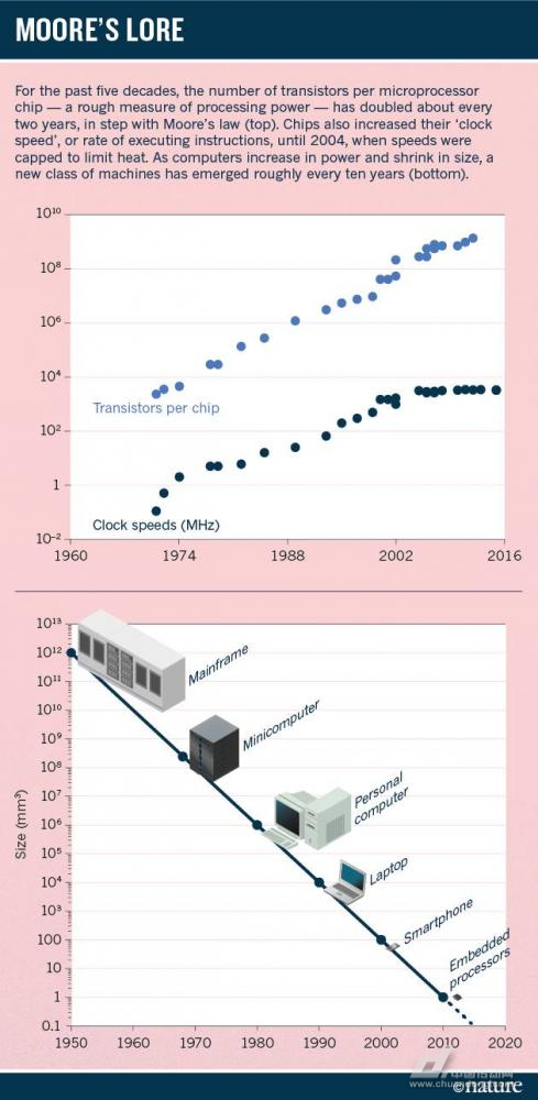
In the 1970s and 1980s, consumer-grade microprocessor devices such as HP computers, Apple II computers, and IBM PCs began to emerge in large numbers. The market demand for such products has also ushered in well blowouts quickly. Manufacturers have participated in this competition and competed to upgrade their chip technology processes.
However, R&D costs are high.
To improve the performance of the microprocessor, it is necessary to scale down the size of the components in the circuit to allow more circuits to be packaged into the chip and thus to speed up the movement of the electrons (processing speed). To reduce the size is bound to need to improve the lithography technology (a basic microprocessor technology to etch on the surface of the silicon).
In the flourishing development period of the chip industry, a natural self-reinforcing cycle ensures that the input-output ratio of chip technology is always in a benign state. Given the wide applicability of chips, manufacturers can only focus on processors and memory technology to ensure that their sales are sufficient to cover the R&D costs for the production of next-generation chips, and that as the technology matures, they can further drive down prices. Drive market demand.
However, it turns out that it is obvious that this market cycle based on Moore's Law has been difficult to sustain.
The complexity of the chip manufacturing process is unimaginable. Hundreds of R&D processes mean that every change of product requires material suppliers and equipment manufacturers to keep pace with the upgrade.
"Assuming that the next generation of chips will require 40 devices to be upgraded, even if only one device is left behind, the entire R&D production cycle will be delayed."
- Kenneth Flamm, computer economist, University of Texas
In order to better plan in the industry, the semiconductor industry has historically designed its own roadmap.
“In this way, every company can have a general plan of what they need to do when they have to, and if anyone has a technical problem, they can give an early warning.â€
- Chairman Gargini of the "Road Map" organization
With the efforts of hundreds of engineers from different companies, the Semiconductor Industry Association of the United States formally launched its first roadmap in its first report in 1991. Gargini, Intel’s director of technology strategy, served as chairman of the association. .

In 1998, with the efforts of all walks of life, associations in Europe, Japan, Taiwan and South Korea began to cooperate with the United States Semiconductor Industry Association to launch the International Technology Roadmap for Semiconductors. With the abandonment of Moore's Law, this year will be renamed the International Roadmap for Devices and Systems.
"The 'road map' is a very interesting experiment. As far as I know, there is no industry that has chosen to bring together manufacturers and suppliers like the chip industry to plan future development together."
- Flamm
In fact, Moore's Law was changed from a rule of thumb to a "natural law" with the help of the "roadmap." In other words, it is precisely because of the “positive response†of the entire industry that the law has become a fait accompli from prophecy.
"In the whole development process, everything seems to be so orderly until it wakes up."
- Flamm
Fever
The first technical bottleneck that will be encountered in the implementation of Moore's Law was already foreseen. Gargini et al. issued a warning as early as 1989.
- In the objective world, "small" is an adjective with limits.
“The previous situation was: Whenever we shrink the size of the process, there will be some good things happen - such as the increase in the speed of the chip processing to reduce the power consumption to provide the corresponding space, which naturally controls the amount of heat. â€
--BillBottoms, President, ThirdMillnniumTestSolutions

However, by the 21st century, when the process technology developed to 90nm or less, this gain effect began to no longer be apparent. Manufacturers have found that the faster electrons run in silicon circuits, the hotter the chips.
This is a basic technical problem.
Although the production of heat is inevitable, no one wants to buy a cell phone for frying eggs.
“Manufacturers eventually chose to seize the only straw — no longer raising the chip's clock speed. This is equivalent to manipulating the chip to limit the amount of heat generated, and this has led to the Since the beginning of the year, there has been no major increase in the frequency of processors."
- Gargini
Not only that, in order to ensure that the performance of the chip can continue to be promoted periodically along with Moore's Law, chip makers have made further efforts to limit the processing speed.
"Although the processing speed is limited, at the same time, chip vendors have redesigned their internal circuits - so that instead of having only one processor in a single chip, they have two, four or even more, and this This is what we now call “multi-core.†Today, quad-core and eight-core have become standard on today’s desktops and smartphones, although theoretically, four 250 MHz chips and a single 1 GHz chip are built in. The processing speed is the same, but in reality, if you want to use 4 processors for co-operation, it means that you need to divide a single task into eight parts, which is very difficult for many tasks. If you can't implement parallel processing on multiple cores, it will instead limit the performance of the chip."
Even so, the combination of the two solutions did help chip makers continue to follow Moore's Law to continue to shrink the circuit size and increase the number of transistors.
However, if you are prepared for peace, due to the quantum effect, the size of the process will inevitably be no longer reduced by the early 1920s. When will the chip industry go?
Perhaps the words of AnChen, an electronic engineer who is an international chip maker GlobalFoundries and chairman of the new roadmap preparation committee, can represent the hearts of chip makers:
"We are still thinking about solutions."
This does not mean that the chip industry does not think about innovation, they also think of a possible solution that can be used - using a new paradigm such as quantum computing and neuromorphic computing.

Quantum computing has the computational potential for exponential growth, while neuromorphic computations can be calculated in the manner of brain-like neurons, both of which have significant computational advantages over traditional silicon processing chips.
However, these alternative paradigms still have a long way to go before they are actually put into commercial production, and many researchers now believe that quantum computing can only have computing advantages in a few niche applications, but it is far from being used in digital computing. Then give power.
Internal upgrade optimization
"As soon as people come out of the technical mindset, they will find that there is still huge research space to be discovered."
- Thomas Theis, physicist at Semiconductor Research Corporation (SRC)
In the digital realm, another solution is to find a “millivolt switchâ€: This material needs to have a computing speed that rivals that of silicon, while also having a lower heat output.
Although there are many candidates for materials, from 2D graphenes to spintronics, all can be calculated by the spin of the electrons instead of the electrons, but at present there is not any kind of millivolt. Switch can really put into commercial use.
Since this method has encountered obstacles, what is the alternative?
So, it was also proposed to improve the architecture: continue to use silicon as raw material, but with a new framework design.
The current popular solution is to build in a 3D manner, that is, to convert the planar etching technology previously performed on the surface of the silicon wafer into a multilayer etching technology, and then stack the thin silicon layers after etching.

Theoretically speaking, this can indeed provide more powerful computing power in the same space. However, in actual operation, it can only be applied to memory chips that do not have heat problems.
This is because the circuit used by the memory chip consumes power only when the memory unit is accessed, and a particular unit is rarely visited frequently, so no excessive heat is generated.
The "hybrid storage cube" design is one such application example - this type of memory stacks up to 8 layers of memory. The design was first promoted by Samsung and Magnesium-led industry associations.
In contrast, it is obviously unscientific to directly apply this design idea to the microprocessor: The more layers that are stacked, the greater the heat output.
However, this problem cannot be solved. The simplest solution is to integrate memory into the microprocessor chip.
After the two are combined, memory and microprocessor chips will no longer need to perform frequent data exchanges, and this can at least kill 50% of the heat. In other words, as long as the memory and microprocessor are integrated into the overlay from the nano level, it can be perfectly solved.
However, it is easier said than done. The first big problem we face is mass production. At present, the structure of microprocessors and memory chips is very different and there is basically no possibility of being produced on the same production line. Not only that, if you want to stack the two organically, you also need to significantly redesign the chip structure. However, in view of the perfection of this solution, there are still many research groups in continuous efforts to try.

Subhasish Mitra, an electrical engineer at Stanford University, and his colleagues have developed a hybrid architecture that can stack memory cells and transistors made of carbon nanotubes and also ensure that electrons move orderly between different overlays. The team also stated that the architecture they designed can reduce power consumption to one thousandth of a standard chip.
The wave of mobile
The second technical bottleneck encountered in the implementation of Moore's Law is almost the same as the first technical bottleneck, but the difference is that this problem is beyond people's expectations, that is, the mobilization of computing.
Twenty-five years ago, the definition of "computing" was limited to desktops and laptops. Even supercomputers or large-scale data centers were, in essence, nothing more than a large number of microprocessors. In the collaborative calculation. However, let's take a look at the present. The daily "calculation" work has been increasingly completed by smartphones and tablets. In addition, wearable devices such as smart watches have further "mobilized" the definition of "calculation." People's demand for these mobile devices is completely different from traditional PCs and laptops, and mobile computing has become a trend.

And in the context of most of today's mobile applications and data processing efforts being handed to cloud servers, these servers will lead chip vendors to continue to follow Moore's Law to launch more powerful microprocessors.
"Google and Amazon's purchasing decisions have a huge impact on Intel's production R&D efforts."
- Reed
However, for mobile phones, more important than performance is the long-lasting endurance.
In a typical smart phone application scenario, the chip must not only be on standby for functions such as voice calls, Wifi, Bluetooth, and GPS, but also provide round-the-clock support for touch sensing, distance sensing, acceleration estimation, magnetic field sensing, and even fingerprint recognition. Therefore, smart phones must have a dedicated power management system to coordinate the circuit power consumption and user experience.
The problem faced by chip makers is that this special demand will undermine the development cycle of Moore's Law self-enhancement.
“In the past, the situation in the market was that even if there were few types of chips, the sales volume of a single product was very large. Now the market is: Even if each chip can only sell hundreds of thousands of chips, chip makers must also Making a wide variety of products requires chip makers to keep design and assembly costs low."
- Reed
Combining many independent production technologies to allow them to work together in the same device is a very difficult task.
"If you want to encapsulate a large number of different material components and electrons, photons, etc., you must develop new architectures that enable coexistence in a confined space, as well as new simulators, switches, etc."
- Reed
For many dedicated circuits, design is still a traditional work that requires a lot of time and manpower.

However, Alberto Sangiovanni-Vincentelli, an electrical engineer at the University of California, Berkeley, and his colleagues are trying to change this situation. The idea is that designers don't need to start from scratch every time they design. They can complete new chip designs by modularly combining a large number of already-designed circuits.
"In theory, this is the same as using LEGO bricks, but this process is also full of challenges, designers need to ensure that these modular circuits can work together. Although the degree of difficulty is relatively large, but always better than Traditional methods for designing circuits are less expensive."
- Sangiovanni-Vincentelli
In other words, the problem plaguing chip vendors today is not technology, but cost.
"The end of the era of Moore's Law is not a matter of technology, but economic issues. At present, chip makers such as Intel are still trying to continue to reduce the size of components rather than looking for solutions from the quantum path. But in fact, the smaller the process size. The higher the R&D cost, this is inevitable."
- Bottom
Each upgrade of the chip process means that manufacturers are creating more precise lithography machines. From the current economic level, the establishment of a new production line usually requires billions of dollars, most companies can not afford to invest so much, and the fragmentation of the mobile device market has further exacerbated the difficulty of returning funds.
"As long as the single-transistor cost required to develop the next-generation chip exceeds the existing cost, this balance will be broken and the upgrade of process dimensions will stop."
- Bottom
Many observers believe that the chip industry is already very close to this critical point.
"I bet we will stop this crazy behavior before we reach the physical limit."
- Reed
Admittedly, rising costs have led to a consolidation wave within the chip industry over the past 10 years. Most of the production lines in the world today are now in the hands of companies such as Intel, Samsung, and TSMC. These chip manufacturing giants have already formed a close united front with equipment manufacturers. The significance of the road map has been greatly reduced.

"The demand for the roadmap by chip makers is no longer strong."
- Vhen
Although SRC is a long-term supporter of the roadmap for the U.S. industry research organization, Steven Hillenius, vice president of SRC, also stated:
"About three years ago, SRC had no longer provided support for the development of the roadmap because internal member companies could not see the meaning of its existence."
A few days ago, together with SIC, SRC began working to establish a longer-term and basic research agenda, and hoped to receive federal funding support in the National Strategic Computing Plan launched in July of last year.
This agenda was put forward in September last year. It contains five reports that describe the research challenges that may face in the future:
The first and foremost is the energy efficiency problem - especially for the "Internet of things" consisting of embedded smart sensors. In the future, it will be necessary to convert the heat and kinetic energy in the surrounding environment into electricity without batteries.
Another issue is connectivity. In the future, the bandwidth required for communications and cloud computing between billions of devices is unthinkable. Currently, one solution that can be foreseen is to use infrared spectrum that is not yet available today. Terahertz band at
The third critical issue is security - in the future we will need to build stronger security mechanisms to guard against cyber attacks and data theft.
Even if only the three points listed above are enough for researchers to work for several years.

However, there are still some people in the industry who are optimistic about this. Among them is Shekhar Borkar, director of advanced microprocessor research at Intel:
"Although literally speaking, the exponential increase in the number of transistors has indeed been unsustainable, and the era of Moore's Law is coming to an end. But from a consumer's point of view, Moore's Law is actually just saying that the value of chips to users is every two years. It will double, and from this point of view, as long as the industry continues to add new features to the equipment, Moore's Law will not die."
In addition, Borkar also said that a specific implementation plan has been released.
"Our mission is to turn these programs into reality.
We've been around for over 16+ years. We make sure our sound is The Best Sound.
Manufacturing high-quality products for customers according to international standards, such as CE ROHS FCC REACH UL SGS BQB etc.
wholesale earbuds, earbuds in bulk, earbuds custom, true wireless earbuds
TOPNOTCH INTERNATIONAL GROUP LIMITED , https://www.micbluetooth.com