FPGA is a field programmable gate array, which is a product of further development based on PAL, GAL, CPLD and other programmable devices. It appears as a kind of semi-custom circuit in the application-specific integrated circuit (ASIC) field, which not only solves the defect of the custom circuit, but also overcomes the shortcomings of the original programmable device with a limited number of gates. This article mainly introduces the FPGA development process and VHDL basic grammar, specifically follow the small series to find out.
Detailed FPGA development process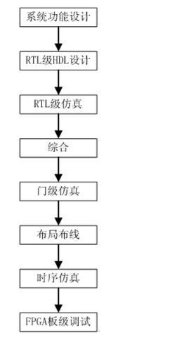
1) System function design
Before the system design, the first thing to do is plan preparation, system design and FPGA chip selection.
In general, a top-down design method is used to divide the system into a number of basic units, and then divide each basic unit into the next level of basic units.
2) RTL Level HDL Design
The RTL level (register transfer level) refers to the details of the register and combinational logic (such as how many logic gates are used, the connection topology of logic gates, etc.), and describes how data flows between registers and how to deal with them. The HDL design method of the model that controls these data flows.
The RTL level is more abstract than the gate level, but it is also simpler and more efficient. The biggest feature of the RTL level is that it can be integrated directly into a gate-level netlist using a synthesis tool, where the RTL level design directly determines the functionality and efficiency of the system.
3) RTL level simulation
Also called function (behavior) simulation, or pre-integration simulation, logic function verification of the circuit designed by the user is performed before compilation. At this time, the simulation has no delay information, and only the preliminary function is detected.
Before the simulation, first use the waveform editor and HDL to create waveform files and test vectors (ie, combine the input signals of interest into a sequence). The simulation results will generate report files and output signal waveforms, and observe the changes of signal at each node. Although simulation is an unnecessary step, it is the most critical step in system design. In order to improve the efficiency of functional simulation, a test platform testbench needs to be established, and test excitations are generally described using behavior level HDL language.
4) Comprehensive
The so-called synthesis is to translate the description of a higher level of abstraction into a lower level of description. Comprehensive optimization optimizes the generated logical connections according to goals and requirements, enabling the hierarchical design to be flat and implemented by the FPGA layout and cabling software.
At the current level, synthetic synthesis refers to the process of compiling design input into logical connected netlists consisting of basic logic elements such as AND gates, OR gates, NOT gates, RAM, and flip-flops. It is not a true gate level. Circuit.
The actual and specific gate-level circuit needs to use the FPGA manufacturer's layout and routing functions to generate the standard gate-level structure netlist generated after synthesis.
5) Gate Level Simulation
Also referred to as post-synthesis simulation, the post-synthesis simulation checks whether the synthesis results are consistent with the original design.
In the simulation, the comprehensively generated standard delay file is back-annotated into the comprehensive simulation model to estimate the impact of the gate delay. However, this step can not estimate the line delay, so there is a certain gap between the actual situation after the wiring, and it is not very accurate. The current synthesis tool is relatively mature, and this step can be omitted for general design. However, if the circuit structure and design intent are found to be inconsistent after layout and wiring, it is necessary to trace back to post-synthesis simulation to confirm the problem.
6) Place and Route
The implementation is to configure the synthetically generated logic netlist onto a specific FPGA chip, matching the logic and timing of the project with the available resources of the device. Layout and routing is the most important process. The layout rationally configures the hardware primitives and the underlying elements in the logic netlist to the inherent hardware structure within the chip, and often requires a choice between speed optimization and area optimization. According to the topological structure of the layout, the wiring utilizes various connection resources within the chip to properly and accurately connect the components. It is also easy to understand the layout as a reasonable configuration of the internal look-up table and register resources of the FPGA. The layout can be understood to pick the optimal combination of resources for the design of the netlist, and the wiring is to maximize the lookup table and register resources. The best way to connect.
At present, the structure of the FPGA is very complex, especially when there are timing constraints, it is necessary to use a timing-driven engine for placement and routing. After the wiring is completed, the software tool will automatically generate a report that provides information on the use of various parts of the design. Since only FPGA chip manufacturers know the structure of the chip best, place and route must choose the tool that the chip developer offers.
7) Timing Simulation
It refers to the back tagging of layout routing information to the design netlist to detect timing violations (ie, timing constraints or device-specific timing rules, such as setup time, hold time, etc.). Timing simulation contains the most complete and accurate delay information, which can reflect the actual work of the chip. Because different internal delays of different chips are different, different layout and routing Solutions also have different effects on the delay. Therefore, after placement and routing, it is necessary to perform timing simulation on the system and each module, analyze its timing relationship, estimate system performance, and check and eliminate competitive risks.
8) FPGA Board Level Debugging
Through the programmer, the layout files are downloaded to the FPGA and their hardware is programmed. The configuration file is usually in the .pof or .sof file format. The download methods include AS (active), PS (passive), and JTAG (boundary scan).

1, reference library
Library IEEE; / / Open the IEEE library, because the IEEE library does not belong to the VHDL standard library, so the contents of the use of the library must first declare
Use ieee.numeric_std.all; //USE and ALL are keywords that allow all the contents of the numeric_std package in the IEEE library to be used. This package is mainly used for data type conversion.
Use ieee.std_logic_unsigned.all;
Use ieee.std_logic_misc.all;
Use ieee.std_logic_1164.all;
Library UNISIM; //UNISIM is a library function of xilinx, used for simulation. In addition to this declaration, you must compile the library and map the library to the simulator.
Use UNISIM.VCOMPONENTS.ALL;
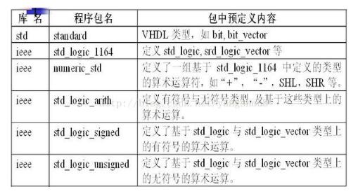
The use of packages can be found in the EDIT-> language templates->VHDL->Common Constructs->Convertion Functions.
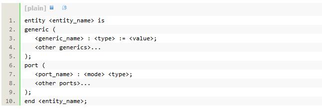
2, entity entity
The entity is similar to a component symbol in the schematic. It does not describe the specific function of the design, but only defines all the input/output signals required.
For example:

EDIT-"language templates-"VHDL-"Common Constructs-"Architecture Components & entity examples
3, structure architecture
All entities that can be simulated are described by ARCHITECTURE, which means that the structure describes the structure or behavior of the entity. An entity can have multiple structures, and each structure represents a different implementation of the entity's function.
The structure name is the name of this structure. It is the unique name of the structure. Although it can be freely named by the designer, the name and the description of the entity are generally combined. The structure has three ways to describe the entity (brackets). Named for:)
1) Behaviour description (BEHAVE): Reflects a design's functions and algorithms, generally using the process PROCESS, expressed in a sequence statement; (in the case of the following example)
2) Structure description (STRUCT): reflects the characteristics of a design hardware, expresses the connection relationship between internal components, and uses component instantiation to describe;
3) DATAFLOW: Reflects the flow of data from input to output in a design, using parallel statement description
For example:
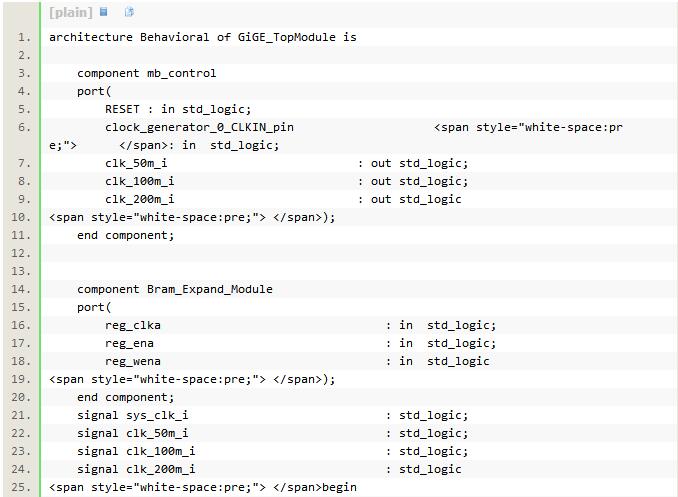
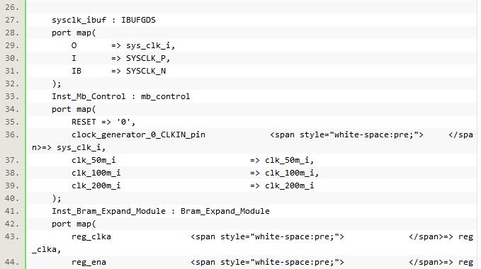
EDIT-"language templates-"VHDL-"Common Constructs-"Architecture Components & entity examples

4, component component
In the above example, there is an instantiation of the component, specifically:

Fttx-The Last Miles,Fttx - Last Mile Networking Solution,Last-Mile Otdr For Fttx Networks Integrates Opm,Last Mile Fttx Test
Huizhou Fibercan Industrial Co.Ltd , https://www.fibercannetworks.com