The AD9854 is available in an 80-pin LQFP package. There are a total of 40 8-bit control registers for controlling the output signal frequency, phase, amplitude, step slope, and some special control bits. The following table shows the distribution of the control registers.
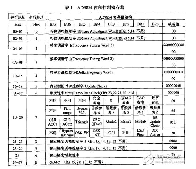
The AD9854 can generate a wide variety of output signals. The selection of the operating mode is achieved by controlling the three bits (Mode2, Mode1, Mode0) in the control register IHF. See the table below.

In fact, in addition to the above-mentioned working methods, more output signal forms (for example, non-linear FM signals) can also be generated through combined control of different working methods. The following are introduced separately.
SingleToneThis is the default operating mode after the AD9854 is reset. The output frequency is determined by the 48-bit frequency tuning word 1 (FrequcncyTuningWordI--FTW) written in the control registers 04H~09H, the phase is determined by the 14-bit phase tuning word in the control register 00H~01H, and the output signal amplitude of the 1 and Q channels. It can be determined by the two 12-bit amplitude adjustment control words in the control registers 21H-22H and 23H-24H, respectively. At this time, frequency tuning word 2 (FTW2, 0AH~0DH) and phase tuning word 2 (02H~03H) are not used.
Frequency tuning word (FTW) = (fout & TImes; 2N)/fsysglk
Among them, fout; output signal frequency (0~fsysglk/2);
N, the resolution of the phase accumulator, here is 48 bits;
Fsysglk, system clock.
It is worth noting that the output of the 1 and Q channels are orthogonal at any time. In addition, all frequency changes are continuous in phase.
Frequency Shift Keying Mode (FSK)The two frequencies F1, F2 are determined by the values ​​in FTW1 and FTW2 respectively, and which frequency is output is determined by the level of Pin29. Pin29 is "0" and output F1; Pin29 is "I" output F2.
Frequency Gradient FSK (RampedFSK)The AD9854 provides a frequency-graded FSK output mode that improves the bandwidth performance of the output signal. The difference between the output filter and the traditional FSK is shown in Figure 1.
At this time, the frequency change from Fl to F2 is not mutated, but gradually changes from F1 to F2 with a certain slaughter. The slope is made up of a 20-bit gradual rate clock (RampRateClock-RRC, 1AH~1CH) and 48-bit. The values ​​in the frequency step word (DetaFrequencyWord--DFW, 10H~15H) register are determined jointly.
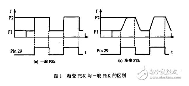
The low frequency control word is set in the FTW1 register, and the high frequency control word is set in the FTW2 register. The duration control word of each intermediate frequency in the ramping process is set in the RRC register. The value in the 48-bit DFW register determines the amount of each frequency step. The increase or decrease in frequency is determined by the level at Pin29. Pin29 is "0", rising: Pin29 is "1", falling. When the end frequency is reached, the ramp is stopped and the end frequency is maintained.
A. Automatic triangular wave frequency output. If the Triangle bit in the control register 1FH is set, the level control on the pin 29 pin is not required and the AD9854 can generate a sawtooth frequency output from F1 to F2 and then immediately from F2 to F1 as set in the RRC and DFW registers. .
B. Control bits CLRACCI (] FH register): When this bit is "1", the current frequency ramping process is stopped, and the next gradual transition process is resumed at the starting frequency.
C. Control bits CLRACC2 (in the 1FH register): When this bit is set to "1", the AD9854 outputs a DC signal (0 Hz).
Two-phase shift keying mode {BPSK)The control of this mode of operation is similar to the FSK mode. The two output phases P1 and P2 are respectively determined by two 14-bit phase adjustment control word registers (00H~01H, 02H~03H); the level at Pin 29 determines which of the two phases is used as the start phase. The annoyance of the output signal is determined by the value in the FTW1 register.
Phase resolution = 360 degrees / 2 to the 14th power = 0.023093791 degrees
Linear FM Mode (FMChirp)The AD9854 generates accurate linear or non-linear FM signals at the user's required frequency resolution, FM slope, sweep direction, and frequency range. At this time, the value loaded in the register FTW1 determines the starting frequency; the frequency step amount is determined by the register DFW; the intermediate frequency duration is determined by the register RRC, Pin29 is the “Hoid†function, and the high-speed Chirp process is paused. The output frequency remains unchanged until Pin 29 goes low again, and the original Chirp process continues with the original slope.
It should be noted that the Chirp mode only specifies the starting frequency and does not set the end frequency, so the user needs to decide when to stop the process. If the stop command is not issued in time, the frequency will continue to rise to fsysglk/2.
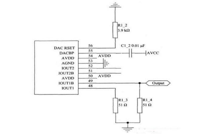
AD9854 Application CircuitThe AD9854 DDS chip is used here. It can generate signals up to 150 MHz according to the Nyquist sampling law when driven by a 300 MHz clock. In order to obtain a better signal frequency, only signals up to 100 MHz are generally obtained. To get a signal higher than 100 MHz, use its higher harmonics. Based on the AD9854 signal generation circuit as shown:
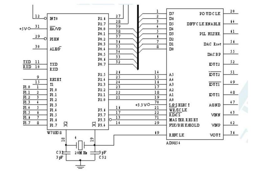
The keyboard has a total of 16 keys consisting of four lines P1.0-P1.3 and four lines P1.4-P1.7. Including the number keys, unit keys and function keys, used to control the frequency, amplitude and function of the desired signal, the final output signal frequency, amplitude and other information through the LCD display. The display part adopts GXM1602NSL LCD module of Guoxian, its core is HD44780. The data transmission with the W78E58 adopts 8-bit parallel transmission and can display 32 lines of characters in two lines. HD44780 supports user-defined characters, so it can be programmed to display Chinese characters and digital information such as frequency, amplitude, and waveform. The communication interface (RS232) is also used in conjunction with the PC. The PC's control commands can interact with the W78E58 via TXD (Pin 10) and RXD (Pin 11) to control the output of the signal source.
Using FPGA to control the AD9854 to generate radar signal source, here we mainly introduce how to use the verilog language (hardware description language) in the FPGA to control the AD9854 to generate a sine wave. Because we adopt the form of SPI bus, it mainly involves the preparation of clock signal, chip select signal and control word of sine wave. Let us first show you the top-level block diagram. We are running under the uartus/'target='_blank'>QUARTUSII8.1 environment. Specifically shown in Figure 1:
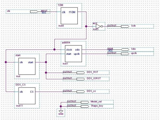
As can be seen from the above figure, the sine wave generated based on the FPGA control mainly includes the following parts:
A: clock frequency division part; B: DDS control signal part; C: AD9854 control word part.
(a) Clock dividerSince we are inputting 50 MHz from the outside, and for the SPI bus, according to its protocol, the clock is typically 100 kHz or 400 kHz, and we use 10 MHZ, which involves a 5-way circuit design. The specific design is shown in the figure below:

The reset signals, mode selection signals, and chip select signals of the AD9854 chip are all included in this section. Here we will directly select the mode selection and waveform keyword signal pins to ground. The AD9854 reset and I/O port reset signals rely on clock signals. The chip select signal is a chip select signal generated by the DDS chip after the clock signal appears for a period of time.
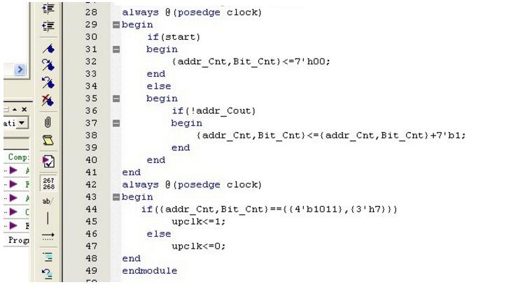
(c) Part of the AD9854 control wordThis part mainly involves how to grasp the timing very well. We store the pre-calculated control in a predetermined memory and read these control words in order through the clock synchronization signal. Specific key parts are shown in the figure below:
60V Battery Pack ,Battery Pack With Outlet,Back Up Battery Pack,Ev Battery Pack
Zhejiang Casnovo Materials Co., Ltd. , https://www.casnovo-new-energy.com