Cypress's FM0-64L-S6E1C3 series is a high-reading integrated 32-bit MCU designed for low-power and low-cost embedded controllers. The device has an ARM Cortex-M0+ processor with integrated on-chip flash and SRAM, and includes Various peripheral functions including various timers, ADCs and various communication interfaces (UART, CSIO (SPI), I2C, I2S, smart card, and USB). The operating frequency is up to 40.8MHz. This article describes FM0-64L-S6E1C3. Main product features, block diagrams, and main features of the FM0-64L-S6E1C3 MCU Starter Development Board, component layouts, system block diagrams, schematics, bill of materials, and PCB design files.
The S6E1C3 Series is a series of highly integrated 32-bit microcontrollers designed for embedded controllers aiming at low powerconsumpTIon and low cost. This series has the ARM Cortex-M0+ Processor with on-chip Flash memory and SRAM, and consists ofperipheral funcTIons such as as various TImers, ADC and communicaTIon interfaces (UART, CSIO (SPI), I2C, I2S, Smart Card, and USB).
The products which are described in this data sheet are placed into TYPE3-M0+ product categories in "FM0+ Family Peripheral Manual".
FM0-64L-S6E1C3 main features:
32-bit ARM Cortex-M0+ Core
ï® Processor version: r0p1
ï® Maximum operating frequency: 40.8 MHz
ï® Nested Vectored Interrupt Controller (NVIC): 1 NMI (non-maskable interrupt) and 24 peripheral interrupt with 4 selectable interrupt priority levels
ï® 24-bit System timer (Sys Tick): System timer for OS taskmanagement
Bit Band Operation
Compatible with Cortex-M3 bit band operation.
On-Chip Memory
ï® Flash memory
ï¯ Up to 128 Kbytes
ï¯ Read cycle: 0 wait-cycle
ï¯ Security function for code protection
ï® SRAM
The on-chip SRAM of this series has one independent SRAM.
ï¯ Up to 16 Kbytes
ï¯ 4Kbytes: can retain value in Deep standby Mode
USB Interface
USB interface is composed of Device and Host
With Main PLL, USB clock can be generated by multiplicationof Main clock.
ï® USB Device
ï¯ USB 2.0 Full-Speed ​​supported
ï¯ Max 6 EndPoint supported
• EndPoint 0 is control transfer
• EndPoint 1, 2 can be selected Bulk-transfer, Interrupt-transfer or Isochronous-transfer
• EndPoint 3 to 5 can select Bulk-transfer or Interrupt-transfer
• EndPoint 1 to 5 consists Double Buffer
• The size of each EndPoint is according to the
• EndPoint 0, 2 to 5 : 64 bytes
• EndPoint1 : 256 bytes
ï® USB host
ï¯ USB 2.0 Full/Low-Speed ​​supported
ï¯ Bulk-transfer, Interrupt-transfer and Isochronous-transfersupport
ï¯ USB Device connected/disconnected automatic detect
ï¯ IN/OUT token handshake packet automatically
ï¯ Max 256-byte packet-length supported
ï¯ Wake-up function supported
Multi-Function Serial Interface (Max 6channels)
ï® 3 channels with 64Byte FIFO (Ch.4, 6 and 7), 3 channelswithout FIFO (Ch.0, 1 and 3)
ï® The operation mode of each channel can be selected fromone of the following.
ï¯ UART
ï¯ CSIO (CSIO is known to many customers as SPI)
ï¯ I2C
ï® UART
ï¯ Full duplex double buffer
ï¯ Parity can be enabled or disabled.
ï¯ Built-in dedicated baud rate generator
ï¯ External clock available as a serial clock
ï¯ Hardware Flow control* : Automatically control the transmission by CTS/RTS (only ch.4)
* : S6E1C32B0A/S6E1C31B0A andS6E1C32C0A/S6E1C31C0A do not support HardwareFlow control.
ï¯ Various error detection functions (parity errors, framing errors, and overrun errors)
ï® CSIO (also known as SPI)
ï¯ Full duplex double buffer
ï¯ Built-in dedicated baud rate generator
ï¯ Overrun error detection function
ï¯ Serial chip select function (ch1 and ch6 only)
ï¯ Data length: 5 to 16 bits
ï® I2C
ï¯ Standard-mode (Max: 100 kbps) supported / Fast-mode (Max 400 kbps) supported.
ï® I2S (MFS-I2S)
ï¯ Using CSIO (Max 2 ch: ch.4, ch.6) and I2S clock generator
ï¯ Supports two transfer protocol
• I2S
• MSB-justified
ï¯ Master mode only
I2C Slave
ï® I2C Slave supports the slave function of I2C and wake-upfunction from Standby mode.
Descriptor System Data Transfer Controller (DSTC)(64 Channels)
DS The DSTC can transfer data at high-speed without going via the CPU. The DSTC adopts the Descriptor system and, following the specified contents of the Descriptor that hasalready been constructed on the memory, can access directlythe memory / peripheral device and performs the datatransfer operation .
ï® It supports the software activation, the hardware activation, and the chain activation functions
A/D Converter (Max: 8 Channels)
ï® 12-bit A/D Converter
ï¯ Successive approximation type
ï¯ Conversion time: 2.0 μs @ 2.7 V to 3.6 V
ï¯ Priority conversion available (2 levels of priority)
ï¯ scan conversion mode
ï¯ Built-in FIFO for conversion data storage (for scanconversion: 16 steps, for priority conversion: 4 steps)
Base Timer (Max: 8 Channels)
The operation mode of each channel can be selected from one of the following.
ï® 16-bit PWM timer
ï® 16-bit PPG timer
ï® 16/32-bit reload timer
ï® 16/32-bit PWC timer
General-Purpose I/O Port
This series can use its pin as a general-purpose I/O port whenit is not used for an external bus or a peripheral function. Allports can be set to fast general-purpose I/O ports or slowgeneral-purpose I/O ports. In addition, this series has a portrelocate function that can set to which I/O port a peripheralfunction can be allocated.
ï® All ports are Fast GPIO which can be accessed by 1cycle
ï® Capable of controlling the pull-up of each pin
ï® Capable of reading pin Level directly
ï® Port relocate function
ï® Up to 54 fast general-purpose I/O ports @64-pin package
ï® Certain ports are 5 V tolerant.
Dual Timer (32-/16-bit Down Counter)
The Dual Timer consists of two programmable 32-/16-bit downcounters. The operation mode of each timer channel can be selected from one of the following.
ï® Free-running mode
ï® Periodic mode (= Reload mode)
ï® One-shot mode
Real-Time Clock
The Real-time Clock countsyear/month/day/hour/minute/second/day of the week from year00 to year 99.
ï® The RTC can generate an interrupt at a specific time(year/month/day/hour/minute/second/day of the week) and can also generate an interrupt in a specific year, in a specificmonth, on a specific day, at a Specific hour or at a specific
Minute.
ï® It has a timer interrupt function generating an interrupt upona specific time or at specific intervals.
ï® It can keep counting while rewriting the time.
ï® It can count leap years automatically.
Watch Counter
The Watch Counter wakes up the microcontroller from the low power consumption mode. The clock source can be selected from the main clock, the sub clock, the built-in high-speed CRclock or the built-in low-speed CR clock.
Interval timer: up to 64 s (sub clock: 32.768 kHz)
External Interrupt Controller Unit
ï® Up to 12 external interrupt input pins
ï® Non-maskable interrupt (NMI) input pin: 1
Watchdog Timer (2 Channels)
The watchdog timer generates an interrupt or a reset when thecounter reaches a time-out value.This series consists of two different watchdogs, hardwarewatchdog and software watchdog.
The hardware watchdog timer is clocked by the built-inlow-speed CR oscillator. Therefore, the hardware watchdog isactive in any low-power consumption modes except RTC, Stop,
Deep standby RTC and Deep standby Stop mode.
CRC (Cyclic Redundancy Check) Accelerator
The CRC accelerator calculates the CRC which has a heavysoftware processing load, and achieves a reduction of the integrity check processing load for reception data and storage.
ï® CCITT CRC16 and IEEE-802.3 CRC32 are supported.
ï¯ CCITT CRC16 Generator Polynomial: 0x1021
ï¯ IEEE-802.3 CRC32 Generator Polynomial: 0x04C11DB7
HDMI-CEC/Remote Control Receiver (Up to 2Channels)
ï® HDMI-CEC transmitter
ï¯ Header block automatic transmission by judging Signalfree
ï¯Generating status interrupt by detecting Arbitration lost
ï¯ Generating START, EOM, ACK automatically to outputCEC transmission by setting 1 byte data
ï¯ Generating transmission status interrupt when transmitting1 block (1 byte data and EOM/ACK)
ï® HDMI-CEC receiver
ï¯ Automatic ACK reply function available
ï¯ Line error detection function available
ï® Remote control receiver
ï¯ 4 bytes reception buffer
ï¯ Repeat code detection function available
Smart Card Interface (Max 1 Channel)
ï® Compliant with ISO7816-3 specification
ï® Card Reader only/B class card only
ï® Available protocols
ï¯ Transmitter: 8E2, 8O2, 8N2
Receiver: 8E1, 8O1, 8N2, 8N1, 9N1
ï¯ Inverse mode
ï® TX/RX FIFO integrated (RX: 16-bytes, TX: 16-bytes)
Clock and Reset
ï® Clocks
A clock can be selected from five clock sources (two external oscillators, two built-in CR oscillator, and main PLL).
ï¯ Main clock: 8 MHz to 48 MHz
ï¯ Sub clock: 32.768 kHz
Built-in high-speed CR clock: 8 MHz
Built-in low-speed CR clock: 100 kHz
ï¯ Main PLL clock 8MHz to 16MHz (Input), 75MHz to 150MHz (Output)
ï® Resets
ï¯ Reset request from the INITX pin
ï¯ Power on reset
ï¯ Software reset
ï¯ Watchdog timer reset
ï¯ Low-voltage detection reset
ï¯ Clock supervisor reset
Clock Supervisor (CSV)
The Clock Supervisor monitors the failure of external clocks with a clock generated by a built-in CR oscillator.
An If an external clock failure (clock stop) is detected, a reset isasserted.
ï® If an external frequency anomaly is detected, an interrupt ora reset is asserted.
Low-Voltage Detector (LVD)
This series monitors the voltage on the VCC pin with a 2-stage mesh. When the voltage falls below a designated voltage, the Low-voltage Detector generates an interrupt or a reset.
ï® LVD1: monitor VCC and error reporting via an interrupt
ï® LVD2: auto-reset operation
Low Power Consumption Mode
This series has six low power consumption modes.
ï® Sleep
ï® Timer
ï® RTC
ï® Stop
ï® Deep standby RTC (selectable between keeping the value of RAM and not)
ï® Deep standby Stop (selectable between keeping the value of RAM and not)
Peripheral Clock Gating
The system can reduce the current consumption of the total system with gating the operation clocks of peripheral functions not used.
Debug
ï® Serial Wire Debug Port (SW-DP)
ï® Micro Trace Buffer (MTB)
Unique ID
A 41-bit unique value of the device has been set.
Power Supply
ï® Wide voltage range:
VCC = 1.65V to 3.6 V
VCC = 3.0V to 3.6V (when USB is used)
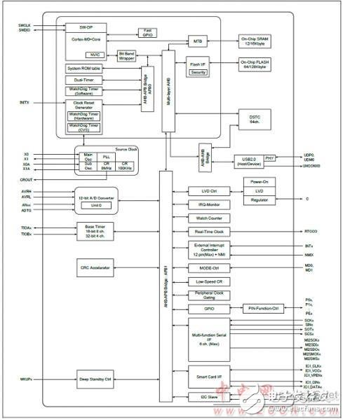
Figure 1. Functional Block Diagram for FM0-64L-S6E1C3
The FM0-64L-S6E1C3 MCU Starter Kit is a low cost development platform for Cypress's FM0+ S6E1C-Series, a Flexible Microcontroller family with an ultra-low-power 32-bit ARM® Cortex®-M0+ CPU. This kit enables rapid development of Embedded systems with onboard interfaces including USB, digital audio and an ArduinoTM Uno-compatible form-factor to prototype with Arduino shields.
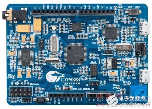
Figure 2. Outline drawing of the FM0-64L-S6E1C3 MCU Starter Development Board
The main features of the FM0-64L-S6E1C3 MCU Starter Development Board:
Featuring the FM0+ S6E1C-Series: ARM® Cortex-M0+ MCU
40MHz ARM® Cortex-M0+ MCU with 64-channel DMA
128KB flash, 16KB SRAM and 54 GPIOs
Industry's most efficient 35μA/CoreMark® Score
Ultra-low-power consumption: Active - 40μA/MHz and Standby - 1.2μA
Advanced peripherals: USB host and device, HDMI-CEC and 6x Serial Interfaces
The FM0-64L-S6E1C3 MCU Starter Development Board includes:
FM0+ S6E1C-Series Starter Board
USB Standard-A to Micro-B cable
Quick Start Guide
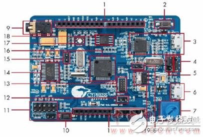
Figure 3. Distribution of major components of the FM0-64L-S6E1C3 MCU Starter Development Board
1. Arduino Interface (CN7-CN10)
2. User button
3. MB9AF312K programmer and debugger (CMSIS-DAP)
4. Serial programming mode select (J3)
5. Power supply resource select (J4)
6. USB device connector (CN4)
7. Potentiometer
8. MB9AF312K programming mode jumper (J1)
9. Headphone and microphone jack (CN1)
10. Reset button
11. Multicon connector (CN12, CN13)
12. Jumper for current measurement (J5)
13. 10-pin JTAG connector
14. Stereo codec
15. Programming mode jumper (J2)
16. Cypress FM0+ MCU S6E1C32D0A
17. RGB LED
18. NOR flash
19. 3.3 V voltage regulator
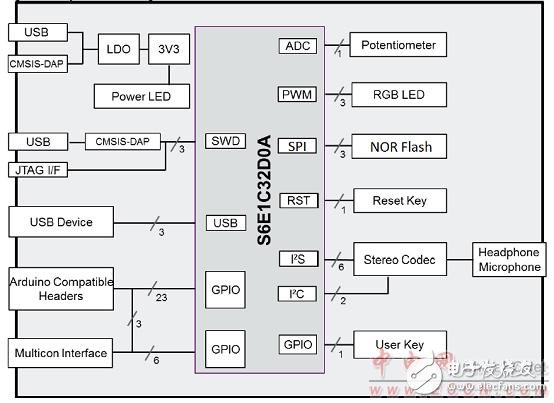
Figure 4. System Block Diagram for Getting Started with the FM0-64L-S6E1C3 MCU
Hardware main features:
 Cypress FM0+ S6E1C-Series MCU
 On-board ICE (CMSIS-DAP compatible)
 USB device interface
 Potentiometer
NOR NOR flash memory
 Stereo codec
RGB RGB LED
 User button
 Arduino compatible headers
 Multicon interface
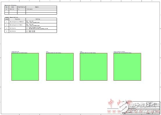
Figure 5. Circuit Diagram for Getting Started with the FM0-64L-S6E1C3 MCU (1)
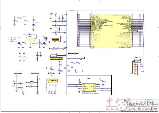
Figure 6. Circuit Diagram for Getting Started with the FM0-64L-S6E1C3 MCU (2)
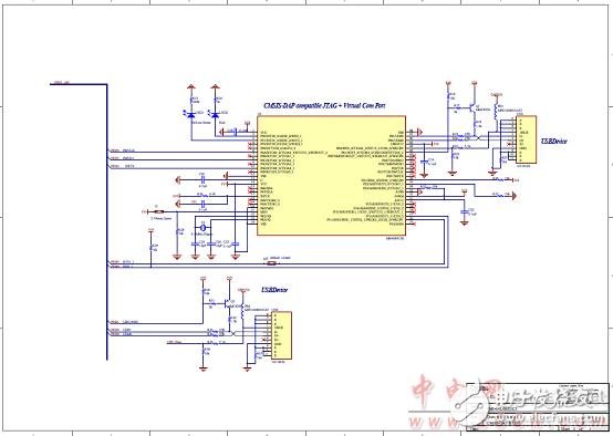
Figure 6. Circuit Diagram for Getting Started with the FM0-64L-S6E1C3 MCU (2)
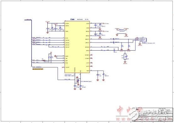
Figure 7. Circuit Diagram for Getting Started with the FM0-64L-S6E1C3 MCU (3)
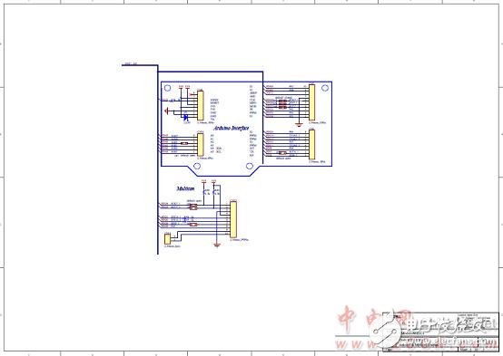
Figure 8. Circuit Diagram for Getting Started with the FM0-64L-S6E1C3 MCU (4)
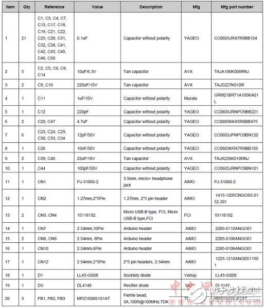
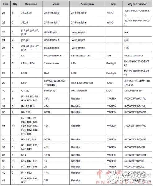
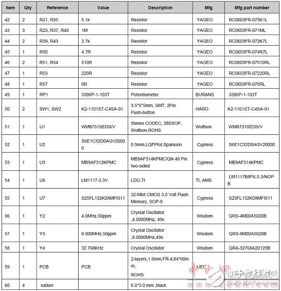
The FM0-64L-S6E1C3 MCU Starter Development Board Bill of Materials:
10-inch tablet devices have greatly surpassed netbooks in terms of entertainment, including reading, games, and audio-visual enjoyment. In other respects, the basic operation of the 10-inch tablet computer built on the touch screen ensures that the application of the tablet computer can be well realized, and its operation performance is closer to that of a smartphone.
1.In appearance, the 10-inches tablet computer looks like a large-screen mobile phone, or more like a separate LCD screen.
2.In terms of hardware configuration, the 10-inches tablet computer has all the hardware devices of a traditional computer, and has its own unique operating system, compatible with a variety of applications, and has a complete set of computer functions.
3.The 10-inches tablet computer is a miniaturized computer. Compared with traditional desktop computers, tablet computers are mobile and flexible. Compared with Laptops, tablets are smaller and more portable
4.The 10-inches tablet is a digital notebook with digital ink function. In daily use, you can use the tablet computer like an ordinary notebook, take notes anytime and anywhere, and leave your own notes in electronic texts and documents.
10 Inches Tablet Pc,Tablet Pc Android,10 Inch Quad Core Tablet,Tablet 10 Inch
Jingjiang Gisen Technology Co.,Ltd , https://www.jsgisengroup.com