Abstract: For the problem of data "bit" in large-capacity solid-state memory, most of the software ECC models are used for error detection and error correction, but this will inevitably affect the read and write performance of the storage system. Based on the ECC verification principle, a parallel hardware ECC model is proposed and implemented by FPGA. Simulation analysis and experimental results show that the model not only has good error correction capability, but also significantly improves the read and write performance of the storage system.
Due to the limitations of the NAND Flash production process, the chip occasionally “bits†flipping during data storage or transmission, requiring necessary error detection and correction. Commonly used data verification methods include parity check and CRC check [1]. However, when a NAND Flash error occurs, it will not cause all the blocks or pages to be wrong, but one or more of them will be wrong. Therefore, the dedicated ECC (Error Checking and CorrecTIng) is often used in NAND Flash processing. Test.
The traditional ECC verification method is generally implemented in software. Although the complexity is low and it is easy to implement engineering applications, since the ECC verification operation is required every time the NAND Flash is read and written, a large number of calculation verification work brings huge software. The overhead directly leads to a decrease in the read and write performance of the storage system.
This paper is based on the hardware structure of high-speed large-capacity solid-state memory [2], combined with the characteristics of NAND Flash full page read and write access [3], using FPGA logic to design and implement hardware, and proposed a parallel hardware ECC model, The ECC checksum data is read and written simultaneously and concurrently, which not only ensures the reliability of the data, but also significantly improves the read and write performance of the storage system.
1 software ECC modelThe ECC check [4, 5] is developed on the basis of parity. It treats the data block as a matrix and generates ECC check codes using the row and column parity information of the matrix. It detects and corrects 1-bit errors and detects 2-bit errors, overcoming the limitations of traditional parity that can only detect odd bit errors, checksums, and error correction.
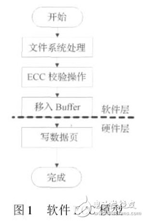
As shown in Figure 1, the working mechanism of the traditional software ECC model is: when the application needs to write data, the file system first processes it accordingly, then generates an ECC check code according to the data to be written, and then checks the data and ECC. The code is moved into the data buffer (hardware buffer), and finally a write command is issued to the hardware controller to write the data to the NANDFlash chip. The process of reading is just reversed.

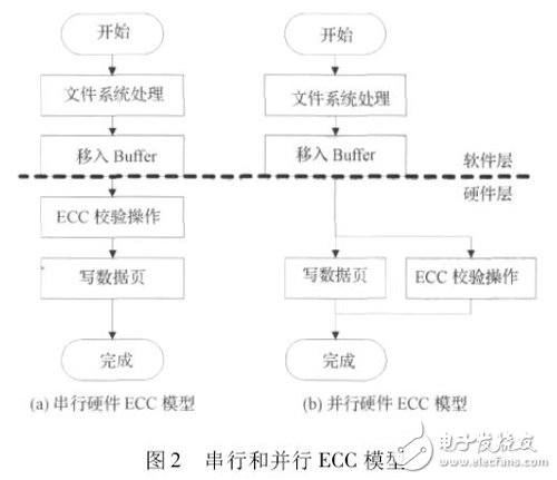
In the software ECC model, the ECC verification operation first brings a huge software overhead, which directly leads to a decline in the read and write performance of the storage system. Second, writing or reading data to the NAND Flash chip is performed in units of pages. Based on these two reasons, this paper proposes a parallel hardware ECC model (referred to as parallel ECC model), as shown in Figure 2 (b). On the one hand, ECC verification is implemented by hardware, which reduces software overhead; on the other hand, the ingenious design of parallel reading and writing of data pages and ECC verification improves read and write efficiency.

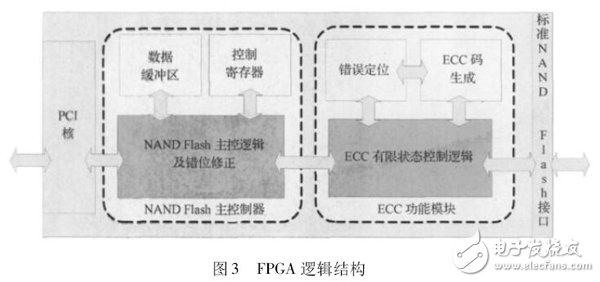
2. 2. 1 FPGA logic structure Large-capacity solid-state memory uses FPGA as the control core. It is composed of multiple NAND Flash memory arrays and uses PCI interface to realize high-speed data transmission. As the control core of large-capacity memory, FPGA has three main parts: PCI core, NAND Flash main controller and ECC function module, as shown in Figure 3. Communication with the CPU and high-speed transmission can be achieved by using the PCI core that comes with Xilinx ISE. The NAND Flash host controller mainly implements timing operations for block erase, page read, page program, ID read, status query, and reset commands of the NAND Flash chip. The ECC function module performs ECC code generation, error detection, and report verification information.

The FPGA logic design must consider not only the timing requirements of the NAND Flash chip for block erase, page read, page programming, etc., but also the read and write access in page units. It also ensures that the ECC function module can correctly detect and correct errors. .
Stage Lights,Beam Lights,Stage Lights,Moving Head Lights
Guangzhou Chengwen Photoelectric Technology co.,ltd , http://www.cwledpanel.com