Abstract: A 16-bit stack processor for embedded control is designed. The processor consists of two stacks: a data stack that executes mathematical expressions and a return stack that supports subroutine calls. The instruction set contains 35 stack instructions. . The architecture and design method of the stack processor are given in detail; not only the simple and effective instruction encoding is used to reduce the code volume, but also the solution to single stack operation of multiple stack elements is given. The processor is implemented in FPGA, and the running clock frequency on the XC5VLX110T chip is up to 146.7MHz. Finally, the software simulation and hardware synthesis results of the design are given.
1 IntroductionForth is a stack-based, extensible, simple philosophical computer programming language [1] invented by Charles H. Moore in the 1960s. It is especially suitable for medium-scale embedded systems with software code in the order of thousands of rows. And it has been widely used in astronomy, military, aerospace, industrial automation, graphics, instrumentation and other fields.
The Forth language can be seen both as an assembly language and as a high-level language. The biggest difference from the traditional language is that it is stack-based and extensible. The Forth language essentially defines a dual stack architecture. The main idea of ​​this architecture is based on two different stacks, one for the data stack that executes the mathematical expression, and one for supporting the subroutine call, that is, the return stack that holds the subroutine return address, the instruction's All operations are for one or several top-of-stack elements of the two stacks [2].
The dual-stack architecture defined by the Forth language is clear and complex, and its main focus is on the field of embedded control. In this context, combined with the flexibility of FPGA, this paper designs and implements an FPGA-based 16-bit stack processor, which has the following advantages compared to the embedded processor based on RISC architecture:
1 largely avoids the overhead caused by the processor to perform context switching, because the operation of the processor does not depend on a large number of general-purpose registers;
2 The addressing mode of the processor is very simple, almost all instructions are 0 operand instructions. In this way, not only the system complexity is significantly reduced, the speed is improved, and the code size is greatly reduced;
3 Processors have a clear advantage when running programs with deep nesting features because of a specialized hardware stack to perform subroutine calls and returns.
2 Design and implementation2.1 Stack Processor Architecture Overview The structure of the processor is shown in Figure 1. In order to clearly show its structure, some signals are not displayed or directly connected. The main modules included in the processor are shown in Table 1.

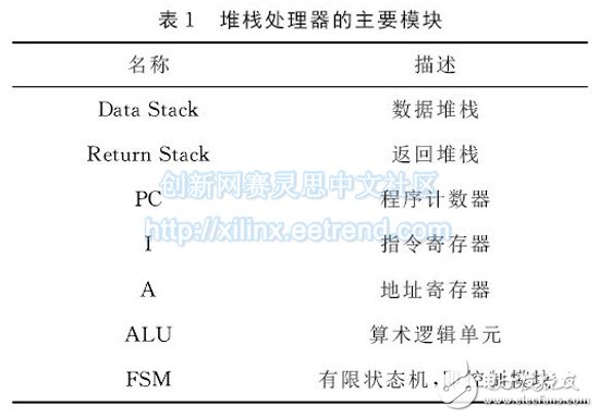
It should be noted that the data stack in the table is composed of a stack top register T, a second stack top register N1, a third top stack register N2, and a stack memory having a depth of 32; the return stack is composed of a stack top register R and a stack having a depth of 32. Memory composition.
2.2 Instruction Set
2.2.1 Instruction Set Design The processor implements a total of 35 instructions in four types, as shown in Table 2 below.
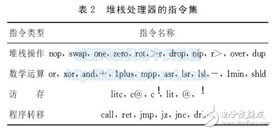
Most of the instructions in the table follow the primitive naming rules and functions of the Forth language. For example, where '>r' means to pop the contents of the data stack top register T to the return stack top register R, 'r>' indicates the opposite function. In addition, '@' means reading data from memory to the data stack, and '! ' indicates that the contents of the data stack are stored in memory. The functions of the various types of instructions are briefly described below.
1 Stack operation : mainly the operation of one or more top elements of the data stack or the return stack. For example, the swap command exchanges the contents of T and N1; the one and zero instructions respectively set all bit positions of T to 1 and 0; the drop instruction pops the contents of T and discards. All stack operation type instructions are completed in one cycle.
2 Mathematical operations : The operands of mathematical operations instructions are the contents of T and N1. The logical operation instructions include or, xor, and and; the shift instructions include asr, lsr, and lsl; 1plus and 1min respectively increment and decrement the top element of the data stack stack by 1. All math type instructions are completed in one cycle.
In order to save hardware resources, the stack processor does not implement hardware-supported multipliers [3] and dividers [4], so there are no direct multiply and divide instructions, instead mpp and shld instructions. These two instructions complete the operation of the multiplier and divider in one clock cycle. The mpp instruction needs to operate the registers T, N1 and N2 at the same time. The initial multiplier and the multiplicand are stored in N1 and N2 respectively, and the initial value of T is 0; the upper and lower 16 bits of the final product result are stored in T and N1, respectively. The execution of the mpp instruction is divided into two steps. The first step is to determine whether the lowest bit of N1 is 1: if it is 1, add N2 and T contents; otherwise, do not operate. In the second step, T is made high and N1 is low, and its content is logically shifted to the right. After 16 consecutive executions of 16 mpp instructions, the T and N1 are respectively stored in the upper and lower 16 bits of the product. These 16 mpp instructions can be combined with several other instructions to complete the normal multiplication operation. The complete multiplication operation takes 19 clock cycles. The division is similar to multiplication, and the complete division operation takes 21 clock cycles. An example of the multiplication operation is given below, and a detailed explanation will be given in the simulation analysis in Section 3.1:
Lect 0 ∥ pushes 0 onto the stack mpp ∥ the first mpp instruction ...
Mpp ∥Article 16 mpp instruction rot ∥ After the multiplication is completed, clean up the drop ∥ the multiplicand at N2
3 Fetching : The stack processor supports both byte and word access. Litc, c@, and c in the instruction set! The instruction is a byte fetch instruction; and lit, @ and ! For memory access instructions. Here is a brief description of the function of the word fetch command, which is similar to byte fetch. Lit pushes a word constant into the data stack; @Press the contents of T to the address register A, press the address in A to fetch the data, and then push it into the data stack; The instruction pops the contents of T into address register A, and then pops the data of the current top T to the address in A. Except for other instructions of the litc instruction that require two cycles of execution, the litc instruction is optimized at design time to not require fetching, so only one cycle is required.
4 program transfer : call is a subroutine call instruction, it will push the current PC register value into the return stack, and send the subroutine address to the PC register; ret is the subroutine return instruction, it will return the stack top value popup, send Into the PC register; jmp is an unconditional jump instruction; jz and jc are conditional jump instructions, the jump condition is whether the content of the top T of the data stack is 0 and whether the ALU carry flag is 0; drjne will return to the stack The content of the top R is decremented by 1, and then it is judged whether the content in R is 0, and if it is not 0, it jumps. All instructions except call and ret need to fetch first to get the 16-bit jump address, and then push it into the stack, so it takes two cycles to execute; the ret and call instructions only need one cycle to execute.
2.2.2 Instruction Set Code Optimization Memory is a scarce resource in embedded control systems. Therefore, when designing the stack processor, a simple but effective coding method is used for instruction coding, which not only greatly reduces the code. Volume, to a certain extent, can reduce the complexity of the system and improve system efficiency.
Programs executing on the stack processor are typically modularized with a large number of subroutine calls to reduce code size in order to take advantage of the hardware-backed return stack. Therefore, 25% of the time in a typical stack processor program is spent on subroutine calls [5], which requires efficient implementation of the call instruction when implementing the stack processor. On the one hand, if the call instruction occupies fewer bits, the code size can be reduced; on the other hand, if the execution of the call instruction can be completed in one cycle, the execution speed of the program will be greatly accelerated. Therefore, the instruction set is implemented in two different encoding methods.
For instructions other than call, each instruction takes 8 bits and the highest bit is 0. Among the 16-bit data accessed by the processor each time, the upper and lower 8 bits are each an instruction. After adopting this design scheme, on the one hand, two instructions can be taken for each memory access. This forms a buffer between the processor and the memory that is twice the speed of the processor, which can avoid the introduction of the Cache to a certain extent and reduce the complexity of the embedded system. On the other hand, each instruction occupies 8 bits. Instead of 16 bits, the code size can be greatly reduced.
The all instruction uses another implementation. If the highest bit of the 16-bit data accessed by the access is 1, then the 16 bits are no longer interpreted as two instructions. The highest bit is interpreted as a call instruction, and the remaining 15 bits are interpreted. The bit is shifted to the left by 1 bit as a subroutine address. This implementation allows the call instruction to occupy only 1 bit, which can further reduce the code size, as opposed to using the same 8-bit implementation as other types of instructions.
In addition, the subroutine address at the time of execution of the call instruction does not need to be fetched, so its execution will only take one cycle. Of course, such a scheme would allow a call instruction to only call a subroutine at an even address, but a good design comes from an appropriate compromise, which is worthwhile relative to the efficiency and performance gains achieved.
Kadena (KDA) is a hybrid blockchain network and smart contract platform that aims to unite public applications, private blockchains, and other interoperable chains in one place, driving traffic to the high-bandwidth computer at the heart of the Kadena public chain. Kadena`s mining algorithm is Blake2S, which supports ASIC mining.
Kadena is a blockchain network and smart contract token aiming to bring together both public applications and private blockchain.
The coin solves various problems that prevent blockchain adoption on a bigger scale. The protocol enables businesses and developers to make transactions and share information across many networks.
The Coin is actually on the grid to reduce users` experience in the network. Ethereum users experience a lot of network congestion which results in high gas fees.
A few changes have come into Kadena mining. A proof of work blockchain uses PACT to create smart contracts in the hidden gen. Therefore you need to know the following before mining Kadena. PACT is an intelligent contract language serving the needs of the blockchain community.
1.You Need an Excellent Mining Hardware
To mine efficiently, you will require suitable mining hardware. Kadena uses ASIC miners. But, unfortunately for Kadena miners, CPUs and GPUs are not usable. Furthermore, ASIC mining receives support from the Blake2S algorithm.
2.Make Sure You Have a Kadena Wallet Address
You will need a Kadena wallet address to receive and monitor your profit. F2pool also makes the distribution of the revenues to every user daily at 2KDA. The Kadena node wallet is a perfect wallet where you can receive your mined KDA. all you need to do is install it, click receive, and have a new wallet address.
You will need to configure your Asic Miner to a mining pool server for your hashrate and profit to be recorded and monitored.
3.Start Mining
After all the setting is done, your miner will be ready to work. Make sure you enter your wallet address and click on the go button to receive your revenue.
Kda Miner,Antminer Ka3 166Th,Bitmain Antminer Ka3 166Th,Antminer Bitmain Ka3
Shenzhen YLHM Technology Co., Ltd. , https://www.sggminer.com