Traffic lights usually refer to traffic lights consisting of red, yellow and green lights that direct traffic. When the green light is on, the vehicle is allowed to pass. When the yellow light is on, the vehicle that has crossed the stop line can continue to pass; when the red light is on, the vehicle is prohibited from passing.
Cross-road vehicles wear combs, pedestrians, bus lanes, pedestrian walkways, and orderly. So what is it to achieve this order? It relies on the automatic command system of traffic lights. There are many ways to control traffic lights. This paper designs a crossroad traffic light control circuit, which requires red, green and yellow traffic lights of east, west and north trunk roads to change cyclically according to requirements, and to indicate the maintenance time of trunk roads or prohibition in countdown mode. And realize the function of the designed circuit on the FPGA experiment board.
1, system overview 1.1, design ideasThe control design of the traffic light system based on FPGA includes four modules, which are pulse generation, state timing, control of traffic light flicker, and control of flicker time. The basic principle is shown in Figure 1.
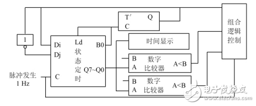
Figure 1 Traffic light control circuit reference schematic
1.2, the overall work situationTraffic light control requirements are shown in Table 1.
The traffic light control of this design is divided into 6 states. Since the duration of each state is different, the core control part of the circuit is a state machine and a timer. The state machine periodically cycles under the trigger of the timer, and the state code controls the six lights to change according to a certain law. The change is shown in Figure 2.
Table 1 Traffic Light Control Requirements
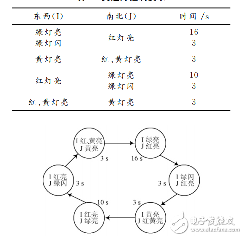
Figure 2 circuit state transition diagram
The system pulse is realized by the FPGA development board crystal oscillator through the frequency division circuit. The state timing is realized by the 74190 reversible decimal counter and the T' flip-flop. As long as the set number is reasonable, the flip signal is in place, so that the circuit can be flipped between the east (I) and north-south (J) control states. The red, yellow, and green flashes are controlled by the 7485 digital comparator and combinational logic, where the 7485 digital comparator is used to compare the current duration of the counter with the desired state all the time and make the corresponding changes. The combinatorial logic control is implemented by writing a truth table from an AHDL file. The time display is implemented by writing the truth table from the AHDL file, inputting the correct logic, and the seven-segment decoding circuit can get the correct time display.
1.3, the composition of each functionThe entire circuit can be divided into 4 major parts, including pulse generation, state timing, time display and digital comparison.
1.3.1, pulse generation
The pulse generator provides the drive for the whole system. When the input is assigned to the PIN55 pin of the FPGA experiment board, the input pulse with a frequency of 10MHz is generated on the experiment board, and 7 pieces of 7490 are used. Each stage constitutes a 10-way circuit. , reducing the frequency from 10MHz to 1Hz.
1.3.2, state timing
The state timing can be implemented by a 74190 cascade of initial values ​​of the preset BCD code to form a down counter. The cascading principle is that the high-order counter can be decremented by one when the low-order counter changes from the all-zero state to the maximum-code-value state. The cascading mode is divided into asynchronous and synchronous. In this paper, the asynchronous cascading mode is adopted, that is, the low-order counter overflow signal controls the counting pulse input terminal of the high-order counter. The high-counter counter can be provided with a valid count pulse edge at the instant when the low-order counter status code changes from all "0" to the maximum code value according to the clock trigger mode of the counter. The specific method is to connect the low-bit overflow signal RCON port to the high-chip count pulse CLK to realize the setting, flipping and borrowing of the two-bit BCD code, so that the number represented by the system can be cycled between 22 and 16.
74190 function description:(1) GN is the counter enable control terminal, active low. When GN is high, counting is disabled.
(2) DNUP is the counting mode control, connected to the high level to reduce the count, and connected to the low level to increase the count.
(3) LDN is asynchronous preset number control. When LDN is low, the counter states QD, QC, QB, and QA are equal to D, C, B, and A, respectively.
(4) The order of the counters from high to low is QD, QC, QB, QA. QD is the highest MSB and QA is the lowest LSB.
(5) The rising edge of the count pulse CLK is valid.
(6) When the counter output QDQCQBQA is the maximum status code "1001" for decimal up counting or the minimum status code for down counting is all "0", the extreme status code indicates that the MAX/MIN output is high.
(7) When the extreme value status code indicates that MAX/MIN is high and CLK is low, the overflow signal RCON is low, that is, RCON is synchronized with the count pulse.
When the system count pulse is 1 Hz, as shown in Table 2, when the timing of the I state (the east-west control state) is 22 s, the counter should first preset the BCD code of 22; similarly, the J state (the north-south control state) should be Preset 16 BCD code.
Table 2 timer counters each state preset number

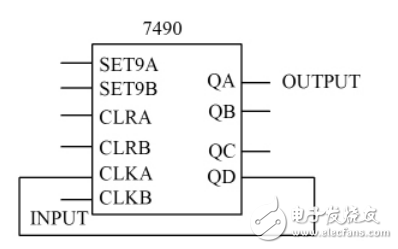
Figure 3 7490 ten-frequency circuit
The state timing circuit is composed of two pieces of 74190 cascaded to form a circuit of 22 and 16 self-reversal. The core issues to be solved include setting, flipping and borrowing. According to the characteristics of the 74190 chip, the implementation principle can be analyzed. As shown in Fig. 4, the borrowing is realized by the rising edge of the overflow signal RCON, so that the number can be borrowed from 20 to 19, and the digits are borrowed from the octet.
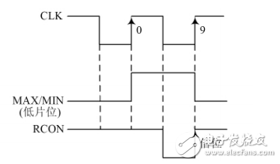
Figure 4 74190 borrowing principle
λ/ 10 - the visible window sheet is a parallel plane plate, which is usually used as a protective film for electronic sensors or detectors in the external environment. We provide flat windows on a variety of substrates without coating and antireflection coating. Antireflective film options include UV, VIS, NIR, and SWIR. Barium fluoride (BaF2), calcium fluoride (CaF2), zinc sulfide (ZnS), zinc selenide (ZnSe) or silicon (SI) germanium (GE) are suitable for infrared applications, while fused quartz and sapphire are suitable for ultraviolet applications.
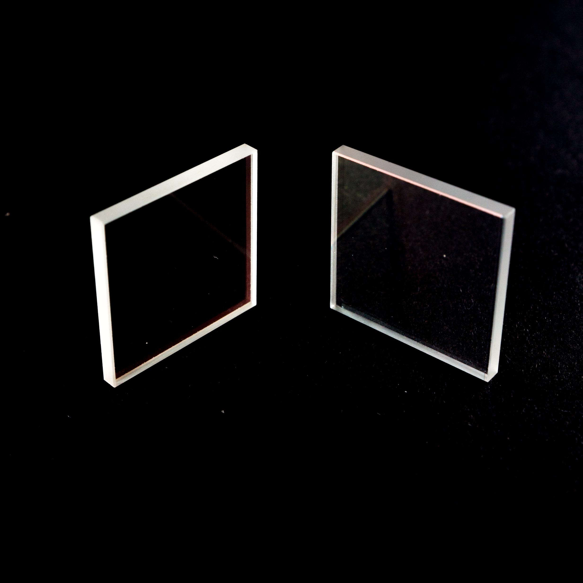
optical windows
Hanzhong Hengpu Photoelectric Technology Co.,Ltd , https://www.hplenses.com