With the rapid development of electronic technology, the variety of electronic devices is increasing. Any electronic device is inseparable from a reliable power supply, and the quality of the power supply is also higher and higher, and the switching power supply has a significant advantage over the conventional transistor linear power supply in terms of efficiency, weight and volume.
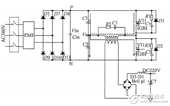
Figure 1 Power main circuit schematic
2, power main circuitThe power module uses a half bridge power inverter circuit. As shown in Figure 1, the three-phase AC power is filtered by the EMI filter, which greatly reduces the electromagnetic interference of the AC power input, and prevents the harmonic crosstalk generated by the switching power supply from being input to the input power terminal. After passing through the bridge rectifier circuit and the filter circuit, the DC voltage is added between the two points P and N. A small-capacity, high-voltage non-inductive capacitor is connected between P and N to function as a high-frequency filter. The half-bridge power conversion circuit is similar to the full-bridge power conversion circuit except that two of the power switching devices are replaced by two capacitors C1 and C2 of equal capacity. In practical applications, in order to increase the capacity of the capacitor and the withstand voltage, C1 and C2 often use a capacitor group composed of a plurality of equivalent capacitors in parallel. The capacity selection of C1 and C2 should be as large as possible to reduce the ripple factor and low frequency oscillation of the output voltage. Due to the limitation on volume and weight, the values ​​of C1 and C2 cannot be infinite. In order to achieve the specified ripple of the output voltage, the capacitance value has a calculation formula, namely:
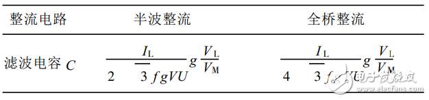
Where, IL is the output load current, VL is the output load voltage, VM is the input AC voltage amplitude, f is the input AC frequency, and VU is the output ripple voltage value.
This is a theoretical calculation formula. The calculated capacitance value that meets the requirements is relatively large. The actual capacitance should be as large as possible. Since the output voltage is small, the capacitance can be increased during the secondary rectification filtering. The capacitance to the formula is not small. Here, C1 and C2 achieve static time division, so that VA = Vin/2.
When VT1 is turned on and VT2 is turned off, the input current direction is the direction of the dotted line in the figure, charging C2, and C1 is discharged through VT1; when VT2 is turned on and VT1 is turned off, the input current direction is the solid line direction in the figure, charging C1 At the same time, C2 discharges through VT2.
When VT1 is turned on and VT2 is turned off, the voltage across VT2 is the input DC voltage Vin. The IGBT's collector-emitter is connected to the RC absorption network to reduce the switching stress of the switching transistor and reduce the peak voltage generated by the IGBT turn-off; the parallel diode realizes the freewheeling effect. The secondary rectification uses a single-phase bridge rectifier circuit to eliminate high-frequency ripple and reduce the low-frequency oscillation of the output DC voltage through the subsequent LC filter circuit. The capacitor in the LC filter circuit is composed of a plurality of high withstand voltage and large capacity capacitors in parallel to improve the reliability of the power supply and make the output DC voltage more stable.
Car Phone Wireless Charging Coil,Circuit Board Induction Coils,Intersection Induction Coils,Induction Coil Set
Shenzhen Sichuangge Magneto-electric Co. , Ltd , https://www.scginductor.com