PCB Layout is an extremely important step in the process of switching power supply R&D. It is related to whether the switching power supply can work normally, whether the production runs smoothly, and whether the use is safe.
Switching power supply PCB Layout is more complex and difficult than other product PCB layouts. There are many more issues to consider and they are summarized in the following aspects:
I. Circuit requirements
1. The components in the PCB must be the same as the BOM.
2. Line traces must conform to the schematic diagram. Using the network connection can do this lightly.
3. The line width must meet the maximum current requirement and must not be less than 1mm/1A to ensure that the temperature rise of the line does not exceed °C.
Reduce the voltage drop sometimes must also widen the width.
4. To reduce the voltage drop and loss, if necessary, tin plating on the line
二.EMI requirements
1. The primary circuit and the secondary circuit are arranged separately.
2. The smaller the area surrounded by the four loops of the AC loop, PFC, PWM loop, rectification loop, and filter loop, the better.
(1) The power components in each loop are as close as possible to each other.
(2) The power lines (between the two AC lines, between the positive line and the ground line) are close to each other.
3. The control IC should be as close as possible to the MOS tube being controlled.
4. The components around the control IC should be placed as close as possible to the IC, especially components directly connected to the IC, such as RT and CT resistors.
The capacitance and correction of the network resistor and capacitor should be arranged near the IC corresponding PIN. The RT, CT to PIN lines should be as short as possible.
5. PFC, PWM circuit to a single point of grounding. IC peripheral components of the first received IC and then connected to the MOS S pole, and then by
The S pole leads to the negative pole of the PFC capacitor.
6. The feedback lines should be as far away as possible from the leads of interference sources (such as PFC inductors, PFC diode leads, MOS transistors), not
Have to run parallel to them.
7. The digital ground should be separated from the simulation ground. The space between ground lines should meet certain requirements.
8. The loop of the bias winding should be directly connected to the negative pole of the PFC capacitor. .
9. The power line (line that flows through a large current) should be short and wide to reduce the loss, increase the response frequency, and reduce the frequency of receiving interference.
Spectral range.
10. In the vicinity of the X capacitor and PFC capacitor pins, the copper strip should be narrowed in order to make full use of the capacitance filtering.
11. Output filter capacitor If necessary, two small capacitors can be used in parallel to reduce ESR.
12. PFC MOS and D, PWM MOS heat sinks must be connected once to reduce common-mode interference.
13. The secondary heat sink and transformer outer shield should be connected to the secondary ground.
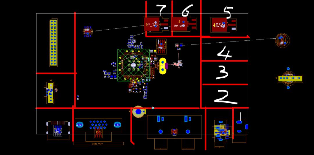
Here we take a graphic processing PCB as an example

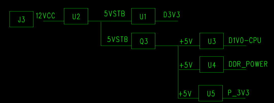
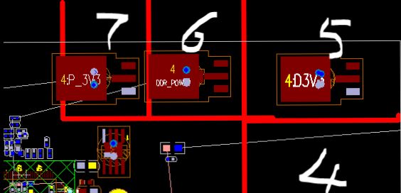
After the decoupling capacitors are placed, it can be seen that all the external interfaces are installed under the PCB. The external power supply is no exception. From the perspective of practicality, we generally choose to place the external power supply in the direction of the interface. It is usually placed in the lower left or right corner of the PCB. In the figure we place the external power supply in the lower right corner of the PCB (area 1). On the right side of the PCB, we have divided the power supply area (1.2.3.4.5.6.7 in the above figure). In general, the order of the power supplies at all levels is arranged in accordance with the figure, and the length of the bus can be reduced. The voltage is also gradually reduced, 12V-5V-3V.

For example, power to the CPU can be placed in this area. Power supply for DDR can be placed in this area 7.

Power supply and power supply components directly follow the principle of proximity. Sometimes there is no way to get close, and it doesn't matter. You can fly. However, it is generally not recommended.
ZGAR AZ MC Disposable
ZGAR electronic cigarette uses high-tech R&D, food grade disposable pod device and high-quality raw material. All package designs are Original IP. Our designer team is from Hong Kong. We have very high requirements for product quality, flavors taste and packaging design. The E-liquid is imported, materials are food grade, and assembly plant is medical-grade dust-free workshops.
Our products include disposable e-cigarettes, rechargeable e-cigarettes, rechargreable disposable vape pen, and various of flavors of cigarette cartridges. From 600puffs to 5000puffs, ZGAR bar Disposable offer high-tech R&D, E-cigarette improves battery capacity, We offer various of flavors and support customization. And printing designs can be customized. We have our own professional team and competitive quotations for any OEM or ODM works.
We supply OEM rechargeable disposable vape pen,OEM disposable electronic cigarette,ODM disposable vape pen,ODM disposable electronic cigarette,OEM/ODM vape pen e-cigarette,OEM/ODM atomizer device.


Disposable E-cigarette, ODM disposable electronic cigarette, vape pen atomizer , Device E-cig, OEM disposable electronic cigarette
ZGAR INTERNATIONAL(HK)CO., LIMITED , https://www.oemvape-pen.com