In recent years, Field Programmable Gate Array (FPGA) has been widely used due to its high performance, low price, high development speed, and convenient programming. However, DPA (DifferenTIal Power Analysis) attacks on FPGAs have become one of the main threats to information security in FPGA applications, and have received extensive attention.
DPA is a kind of SCA (Side Channel Attacks) technology. The attack idea is: based on the power consumption characteristics of the circuit, using the relationship between power consumption and internal key, a large amount of samples will be included in the internal secret. The power waveform data of the key operation is divided according to the guessed key, so that the divided two parts have different power consumption characteristics. Finally, subtract the power consumption data from the two parts to get the power difference curve. If the guess is correct, the differential curve will show obvious spikes.
Therefore, the root cause of DPA attacks is caused by the asymmetry of the circuit logic representation. This paper will apply the FPGA's own structural characteristics, combined with the commonly used circuit-level protection technology against DPA attacks, and deeply research and analyze the circuit-level protection technology for DPA attacks on the FPGA platform.
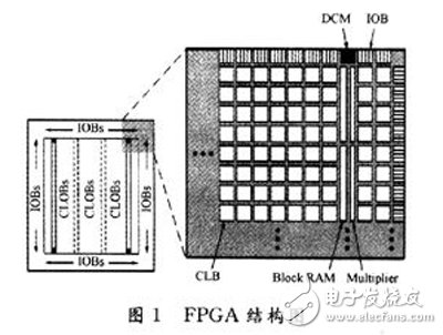
1 Circuit protection technology on FPGA 1.1 The underlying structure of FPGAThe simplified structure of the FPGA is shown in Figure 1. The most important components in FPGA design and design engineering are CLB (Configurable Logic Block), IOB (Input/Output Block), Block RAM (Block RAM), and DCM (Digital). Clock Manager, Digital Clock Manager) and MulTIplier (Multiplier). Among them, CLB is the main bearer of FPGA with programmable capability. The main components of a slice of Virtex-5 include four 6-input lookup tables, four flip-flops and several selectors.
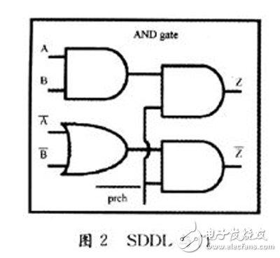
Dual-track circuit technology means that both input and output are represented by two lines. As can be seen from Fig. 2, in the SDDL AND gate, the signal A is represented by A and the common, and the output Z is also represented by Z and. In this representation, a variable can have 4 different logical values ​​(0,0), (0,1), (1,0), and (1,1). SDDL uses (0, 1) and (1, 0) to represent logic 0 and logic 1, respectively. Thus, the logic 0 and logic 1 inside the circuit become symmetrical, so that the respective power consumptions are the same. In addition, the logic gate also introduces a prch precharge signal. In the case where prch is valid, the output is (O, 0), which is the representation of the variable in the circuit when pre-charging. The operation of the circuit is divided into two states: the operational state and the precharge state. These two states are alternately replaced, that is, a fixed period pulse is loaded on the prch. As a result, the change in the value of the variable in the circuit is (0, O) to (O, 1) or (1, O), or (0, 1) or (1, 0) to (O, 0), each The second flip is that only one signal line is flipped. Logic O and Logic 1 reach a complete balance.
1.3 Implementation of pre-charging technologyA normal logic gate cannot provide continuous conversion activity, and the input of the logic gate will cause the data of the gate to be independent. To solve this problem, the conversion is provided by adding a precharge circuit. When the clock is high, the pre-charge circuit is connected to input a pre-charge phase, and the connection point changes to logic O; when the clock is low, the circuit input calculates the phase, and the actual calculation is completed. The purpose of using precharge logic on the FPGA is to require that the output of the slice must be logic 0 during the precharge phase, in two ways. In a Xilinx slice, each LUT is followed by a dedicated multiplexer and memory unit that can be configured as a register or latch. Consider using multiplexers and memory cells to implement pre-charging, each with its own advantages and disadvantages:
(1) A clocked multiplexer is used to implement the precharge function. A separate memory unit in each slice is used as a register, but a reverse clock is assigned to the normal clock of the register. The disadvantage of this method is that copying a clock signal and generating direct and complementary signals will significantly increase power consumption and circuit area, and wiring will also be complicated.
(2) Use the memory unit as an asynchronous clear latch with a reverse enable input to implement the precharge function. Only a single signal is required for the registers and precharge latches. The precharge function is implemented by the clear input that connects the reverse enable input and the latch. The disadvantage of using this method is that the specially designed register memory requires a separate register. Slice.
2 DES encryption module implementationA safety shield is implemented on the FPGA to ensure constant power consumption of critical components. Here we choose to implement bypass security logic on the FPGA from dual-rail and pre-charge technology. Current state of the art requires precise control of placement and routing on the FPGA. The implementation of the DES encryption module based on FPGA is introduced from the implementation of S-box hardware macro and the implementation of DES encryption core.
2.1 S-box hardware macro implementationThe design of the S-box is a key part of the DES algorithm, and the advantages and disadvantages of the S-box design will affect the performance of the entire algorithm. In the implementation of FPGA, from the perspective of resources and speed, the FPGA configurable properties should be effectively utilized, and the internal structure of the device should be fully considered to make both of them as optimal as possible. In the design, due to the intervention of the integrated tools, the output netlist is difficult to be understood by the designer, and at the same time to find a better way to control the combined circuit, so to establish a hardware macro module, referred to as hard macro. This differs from the traditional design flow in that it takes full advantage of the FPG Editor's functionality to achieve dual-track and pre-charge technology from the FPGA infrastructure configuration.
Aluminum Alloy LED lamps,LED Panel light,Led panel light with full color display
Kindwin Technology (H.K.) Limited , https://www.ktlleds.com