IR's IR2110 chip is a monolithic integrated driver module for dual-channel, gate-driven, high-voltage, high-speed power devices. Due to its small size, low cost, high integration, fast response, high bias voltage and strong driving capability, this bootstrap integrated circuit for power MOSFET and IGBT drive has been adjusted since the introduction. Widely used in power drive fields such as speed and power conversion. The IR2110 uses advanced bootstrap circuitry and level shifting technology to greatly simplify the control requirements of logic devices for power devices, allowing each pair of MOSFETs (upper and lower) to share a single IR2110, and all IR2110s can share an independent power supply. For a typical 3-tube three-phase bridge inverter, three IR2110s can be used to drive three bridge arms, requiring only one 10V to 20V power supply. In this way, the volume of the drive circuit and the number of power sources are greatly reduced in engineering, the system structure is simplified, and the system reliability is improved.
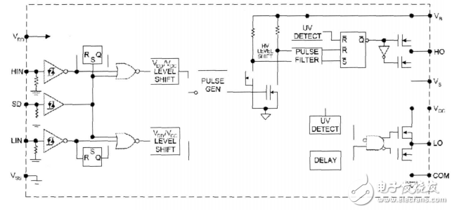
1. Internal structure and functional characteristics of IR2110The IR2110 floating power supply uses a bootstrap circuit with a high-end operating voltage of 500V and an operating frequency of 500kHz. The internal structure is shown in Figure 1. It consists of three parts: logic input, level shifting, and output protection. The IR2110 is fabricated in a CMOS process and has a logic supply voltage range of 5V to 20V. It is suitable for TTL or CMOS logic signal inputs. It has independent high-side and low-side 2 output channels, and both channels have hysteresis undervoltage lockout. Since the logic signals are connected to the respective channels through the level coupling circuit, the logic circuit reference ground (Vss) and the power circuit reference ground (COM) have an offset of 5V, and can shield pulses of less than 50 ns, More ideal anti-noise effect.

Figure 1 IR2110 internal structure
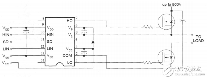
The bootstrap circuit of IR2110 is especially suitable for various bridge driver circuits. The typical application is shown in Figure 2. Pins 3 (VCC) and 6 (VB) are the low-side supply voltage and the high-side floating supply voltage, pin 2 (COM) is the low-side power supply common, and pin 5 (Vs) is the high-side floating power supply common. Pin 9 (VDD) is the logic supply voltage, pin 13 (Vss) is the logic circuit ground, and pin 11 (SD) is the input signal shutdown. VCC is a 10V~20V power tube gate driver. Since VSS can be connected to COM, VCC and VDD can share the same typical power supply with +15V.

Figure 2 IR2110 typical application circuit
When the input logic signal HIN/LIN=1, the output signal HO/LO=1, the control MOSFET is turned on; when HIN/LIN=0, HO/LO=0, the control MOSFET is turned off, and its SD input can be used to block This two-way drive. If the two driving voltages are less than 8.3V, the output signal will be blocked on-chip due to undervoltage. The output gate drive voltage ranges from 10V to 20V, and its typical level conversion time is: Ton=120ns, Toff=94ns. The typical dead time is 10ns. The built-in dead-band circuit prevents the straight-arm conduction caused by the turn-off delay of the MOS device and improves the reliability of the system.

10 Port Usb Charger,10 Port Usb Charging Hub,120W Higher Power Charger,Multi Port Usb Charging Station
shenzhen ns-idae technology co.,ltd , https://www.best-charger.com