An analog-to-digital converter, or A/D converter, or ADC for short, usually refers to an electronic component that converts an analog signal into a digital signal. A typical analog to digital converter is a digital signal that converts an input voltage signal into an output. This article describes the circuit principle of several analog-to-digital converter chips.
1, AD9280
The AD9280 device is a single-chip, 8-bit, 32 MSPS analog-to-digital converter (ADC) that introduces the AD9280's features, application range, reference design circuitry, and circuit analysis to help you reduce design time.
Introduction to AD9280:
The AD9280 is a single-chip, 8-bit, 32 MSPS analog-to-digital converter (ADC) that operates from a single supply and includes an on-chip sample-and-hold amplifier and voltage reference. It features a multi-stage differential pipeline architecture with data rates up to 32 MSPS and guaranteed no missing codes over the entire operating temperature range.
AD9280 features:
Pin compatible with the AD876-8
Power consumption: 95 mW (3 V power supply)
Operating voltage range: +2.7V to +5.5V
Differential Nonlinearity (DNL) error: 0.2 LSB
Power saving (sleep) mode
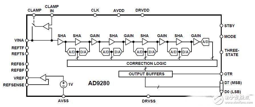
The internal block diagram of the AD9280:

Figure 1 shows the internal structure of the AD9280, showing the internal structure.
AD9280 Reference Design Circuit:

Figure 2 AD9280 typical application circuit
2, AD7541
The AD7541 device is a low cost, high performance 12-bit single-chip multiplying digital-to-analog converter that introduces the AD7541 features, application range, reference design circuitry, and circuit analysis to help you reduce design time.
Introduction to AD7541:
The AD7541A is a low cost, high performance 12-bit single-chip multiplying digital-to-analog converter. The device is fabricated on advanced low noise thin film CMOS technology and is available in standard 18-pin DIP and 20-lead surface mount packages. The AD7541A is functionally and pin-compatible with the industry-standard device, the AD7541, and has improved specifications and performance. In addition, the device design is improved to ensure that latch-up does not occur, so there is no need to output a Schottky diode.
AD7541 features:
Improved version of the AD7541
Complete four-quadrant multiplication
12-bit linearity (end point)
All devices are guaranteed to be monotonic
TTL/CMOS compatible
low cost
No need to protect Schottky diodes
Low logic input leakage
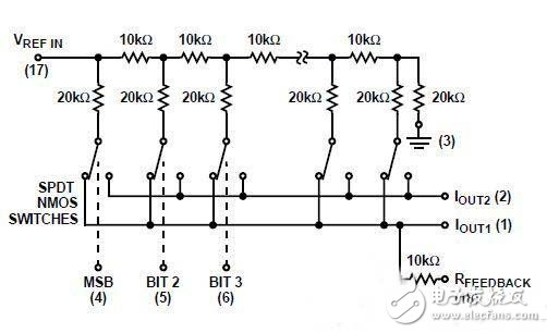
Block diagram of the internal structure of AD7541:

Figure 3 shows the internal structure of the AD7541, showing the internal structure.
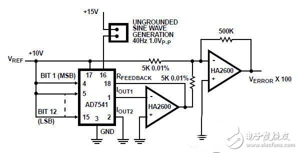
AD7541 Reference Design Circuit:

Figure 4 AD7541 typical application circuit
3, AD7694
The AD7694 device is a 3-channel, low noise, low power, 24-bit sigma-delta ADC with an on-chip instrumentation amplifier that introduces the AD7694 features, application range, reference design circuitry, and circuit analysis to help reduce design time. .
Introduction to AD7694:
The AD7694 is a 16-bit, 250 kSPS, charge redistribution, successive approximation analog-to-digital converter (ADC) that operates from a single 2.7 V to 5.25 V supply (VDD). The device includes a very low power, high speed, 16-bit no-signature sampling ADC (Class B), an internal conversion clock, and an SPI-compatible serial interface port. It also integrates a low noise, wide bandwidth, and very short aperture delay. Sample and hold circuit. On the rising edge of CNV, the AD7694 samples the analog input voltage difference between IN+ and IN-, ranging from 0V to REF. The reference voltage (REF) is supplied externally and can be set to the maximum supply voltage.
AD7694 features:
16-bit resolution
Throughput: 250 kSPS
Integral Nonlinearity (INL): Maximum ± 4 LSB
Power consumption:
800 μA @ 5V/100 kSPS
540 μA @ 2.7V/100 kSPS
Pseudo-differential analog input range: 0 V to VREF (VREF up to VDD)
AD7694 application:
Battery powered device
Medical equipment
Mobile communication
Personal digital assistant
data collection
Instrumentation
Process control
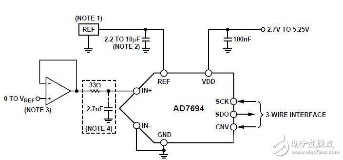
AD7694 reference design circuit:

Figure 5 AD7694 typical application circuit
Edit Comment: This article mainly introduces the AD9280, AD7541 and AD7694 features, application range, reference design circuit and circuit analysis to help you shorten the design time. The AD9280 is a single-chip, 8-bit, 32 MSPS analog-to-digital converter (ADC) that operates from a single supply and includes an on-chip sample-and-hold amplifier and voltage reference. The AD7541A is a low cost, high performance 12-bit single-chip multiplying digital-to-analog converter. The AD7694 is a 16-bit, 250 kSPS, charge redistribution, successive approximation analog-to-digital converter (ADC) that operates from a single 2.7 V to 5.25 V supply (VDD).
Electronic enthusiast "Smart Industry Special", more quality content, download now 
Shenzhen Chaoran Technology Corp. , https://www.chaoran-remote.com